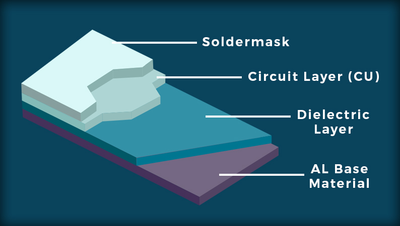
A dielectric layer is sandwiched between every two conductive layers of the Printed circuit board, either the signal layer or the planar layer. For PCBs, the main function of the dielectric layer is support the whole pcb circuit board structure, and the main electrical function is insulation among conductive layers.

First of all, since the thickness of each conductive layer is usually only 36 μm (the thickness of a mass of 1 oz and a density of 8.9 g/cm 3 of copper laid on an area of 1 square foot), Such a thin conductor layer is curled as long as the external force is slightly applied, so the conductive layer cannot support the geometry of the printed circuit board, and it is not possible to provide a position for the components on the board.
At the same time, if the two conductor layers are directly pressed together, the conductors belonging to different networks in the two layers are short-circuited, so an insulating dielectric layer must be added between them. In addition, the dielectric layer also affects the characteristic impedance and energy loss of the transmission line in the conductor layer, and the propagation speed of the signal (parameters required to calculate the parallel signal delay)


