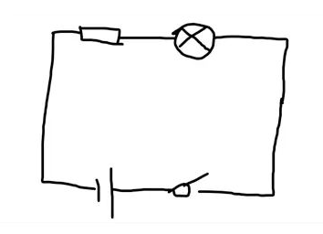
What is Printed Circuit Board Schematic Diagram? Hey, here’s a simple schematic diagram. We can see that the entire circuit loop consists of a dry battery, a switch, a resistor, and a small light bulb, just like the circuit diagram on the junior high school physics textbook.

simple schematic diagram
Instead of actually drawing a light bulb or a battery, we replaced them with simple abstract symbols. Yes, the schematic diagram (Schematics, also denoted by SCH) is a drawing in which the circuit symbols are connected to each other to reflect the electrical connection of the components. It is also a circuit diagram consisting of a simple illustration.
In the actual engineering project, the circuit schematic and the printed circuit board (PCB) are one-to-one correspondence, and one schematic diagram corresponds to one printed circuit board.
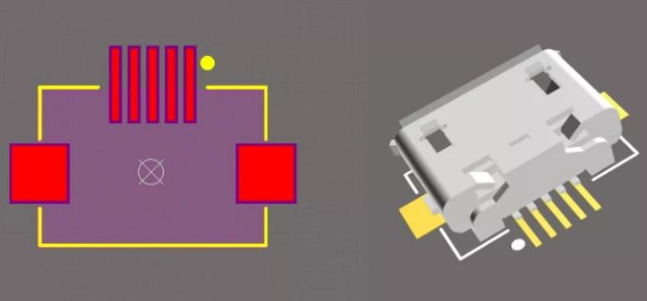
We see that the schematic of above Figure is square, even the size of the switch and the bulb are the same. If you look at the schematic diagram and start soldering components of different sizes on the printed circuit board, you will definitely have problems. So, we need something that can represent the appearance of the component – the package, which describes the shape and size of the components and the arrangement of the pins.

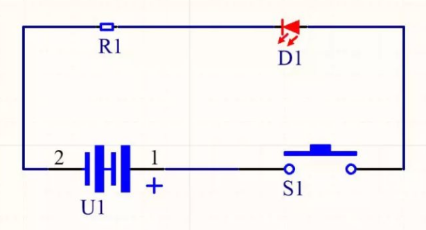
We use a certain icon to redraw the hand-drawn schematic of Figure 1, and we get the following image.

Therefore, according to the electrical connection relationship of each component in the printed circuit board schematic diagram, and then refer to the package information of the component, the entire printed circuit board can be drawn, which is also quite important for PCB reverse engineering.


