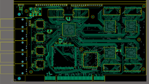
What is difference between PCB Board Schematic & PCB Board Layout Design, the printed circuit board schematic diagram is a simple two-dimensional circuit design that shows the functionality and connectivity between different components. The PCB layout design is a three-dimensional layout, and the position of the components is marked after the circuit is guaranteed to work normally.

What is difference between PCB Board Schematic & PCB Board Layout Design
Therefore, the PCB schematic is the first part of designing a printed circuit board and the last step when reverse engineering PCB board. This is a graphical representation that uses agreed symbols to describe circuit connections, whether in written form or in data form. It also prompts the components to be used and how they are connected.
As the name suggests, the PCB schematic is a plan and a blueprint. It doesn’t indicate where the components will be specifically placed. Rather, the schematic outlines how the PCB will ultimately achieve connectivity and forms a key part of the PCB reverse engineering planning process. After the blueprint is completed, the next step is the PCB design.

The design is the layout or physical representation of the PCB schematic, including the layout of copper traces and holes
The design is the layout or physical representation of the PCB schematic, including the layout of copper traces and holes. The PCB design shows the location of the aforementioned components and their connection to copper. PCB design is a stage related to performance. Engineers built real components on the basis of PCB design so that they can test whether the equipment is working properly. As we mentioned earlier, anyone should be able to understand the PCB schematic, but it is not easy to understand its function by looking at the prototype. After these two stages have been completed, and you are satisfied with the performance of the PCB, you need to implement it through the manufacturer.


