Power integrity is an increasingly complex issue in electronic vehicle PCB board design. A few years ago, all integrated circuits including microprocessors operated at 5V, and you only needed a 5V power supply and ground plane to provide adequate and stable power to the components.
Today, Integrated circuits can operate in multiple voltage modes, down to 0.9 volts. Therefore, a single printed circuit board requires multiple complex distribution grids to supply these voltages and grounds.

Power integrity is an increasingly complex issue in electronic vehicle PCB board design. A few years ago, all integrated circuits including microprocessors operated at 5V, and you only needed a 5V power supply and ground plane to provide adequate and stable power to the components
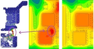
To save costs, computer-aided designers have had to fit these multiple power distribution networks (PDNs) into as few ground planes as possible. The result could be a distribution network like Figure, with a very tight interior (neck undulation), but the need to supply high levels of current to the IC.
The cramped space can lead to serious reliability problems that may not manifest for several years. Excessive current can increase the temperature of the space, which can cause the PCB to burn out like a fuse or explode the circuit board. These distribution networks can now be analyzed in software, and virtual prototypes and high-level current density spaces can be determined. Designers can then expand the space or create parallel current paths in adjacent layers to address this issue while maintaining adequate current supply to the IC.
It is not practical to test the current density problem by using a physical prototype in a test room, as it may take several years to cause a failure. And the problem may never manifest, leading to subsequent failures in this area.


