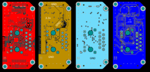
Value Engineering of PCB Cloning
Value Engineering objective
A value engineering (VE) review of PCB Cloning candidates may reveal cost drivers over and beyond the sole source restrictions. Some probable high cost drivers are: excessive material requirements such as the capacitor, resistor, inductor and integrated circuits, PCB layout drawing defects, over design, functional redundancy, tolerance restrictions, excessive performance requirements, etc.
When these or similar conditions are noted, consideration should be given to performing value engineering studies prior to the completion of PCB Cloning process..
Documented results
The results of all studies conducted should be documented in a format suitable to support the inclusion of the dollars saving into the Value Engineering of PCB Cloning accountability system. The documentation should include, as a minimum, the following:
- Originating individuals name, title, signature, official symbol and phone number
- Item, component or part studied,
- National/Federal Stock Number,
- Major end item/system/program,
- Appropriate code & program element, and
- Results from the five phases of the VE job plan:

Value Engineering of PCB Cloning
(1) Information phase,
(2) Function phase,
(3) Speculation phase,
(4) Evaluation phase, and
(5) Development phase.
Estimated cost of change(s) recommended
Estimated net savings to the government
Unit savings
A cost analysis summary to support the above asterisked items.
Logistics support analysis/record
Manual reviews
Manuals should be reviewed and changes resulting from the creation of the technical data package should be incorporated.


