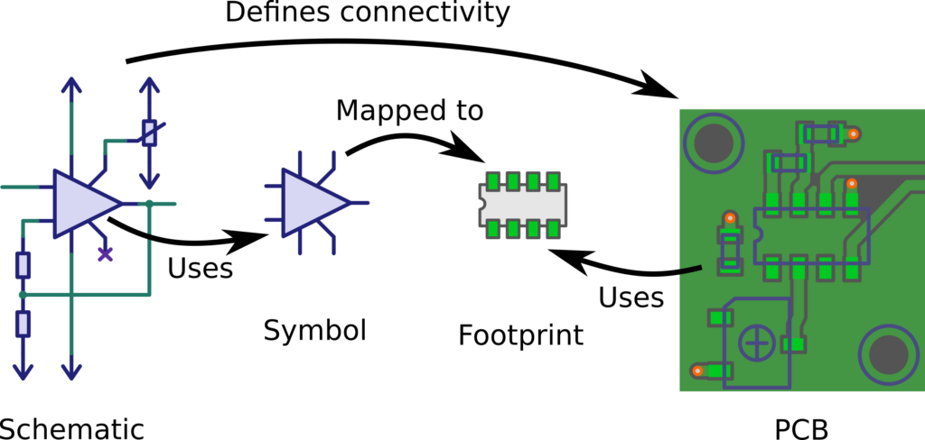
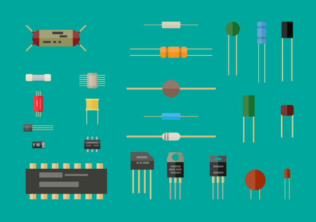
In the Printed Circuit Board Cloning system, the symbol map of the component is represented by a vector diagram. The reason is that in the system, a symbolic diagram is used to represent a type of component. For different pin counts, the chip or component is placed on the printed circuit board in different positions, and the component symbol map is also deformed. Therefore, it can’t be represented by a single bitmap. For example, a chip may have different pin count, so a chip bitmap cannot be used to directly represent a chip. For a two-leg component, although different components are the same amount of pins, the size may be different.

The distance between the pin point and the solder joint is not the same, so the drawing will be different too, it is obviously not possible to use the bitmap. However, the figure is the same for through hole and soldering pad, and the application of vector graphic in the circuitry diagram acquired from pcb reverse engineering technique is too monotonous, and it is more suitable to use the bitmap.

Therefore, when arranging and layout the components on the circuitry diagram, the drawing of the component graphics should be appropriately adjusted according to the number of pins and the placement position. When drawing component graphics on the diagram, various basic graphics should be considered as an object, such as lines, polylines, circles, arcs, ellipses, Bezier curves, text, and so on. Then, some basic graphic objects needed can be combined and defined as primitive objects, and various primitives are classified and organized to form a primitive library for the subsequent component connection processing in PCB board reverse engineering.
When drawing graphics, you can combine various primitives and basic graphics in the library to improve the efficiency and reusability of generating graphics and graphic parameter analysis.


