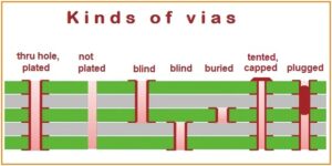
Through Hole in the PCB Board Layout Reverse Design is playing an critical role, from a design point of view, a via is mainly composed of two parts, one is a drill hole in the middle, and the other is the pad area around the drill hole. The size of these two parts determines the size of the via.
Obviously, in high-speed, high-density PCB layout reverse design, designers always hope that the smaller the via, the better, so that more wiring space can be left on the board. In addition, the smaller the via, the parasitic capacitance of its own The smaller, the more suitable for high-speed circuits.

Through Hole in the PCB Board Layout Reverse Design is playing an critical role, from a design point of view, a via is mainly composed of two parts,
However, the reduction of the hole size also brings an increase in cost of PCB manufacturing, and the size of the via hole cannot be reduced without limit. It is limited by drilling and plating (plating) and other process technologies: the smaller the hole, the more The longer the hole takes, the easier it is to deviate from the center position; and when the depth of the hole exceeds 6 times the diameter of the drill hole, there is no guarantee that the hole wall can be evenly plated with copper.
For example, the thickness of a normal 6-layer PCB board (through-hole depth) is about 50Mil, so the minimum drilling diameter that PCB manufacturers can provide is only 8Mil.


