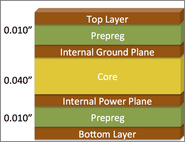
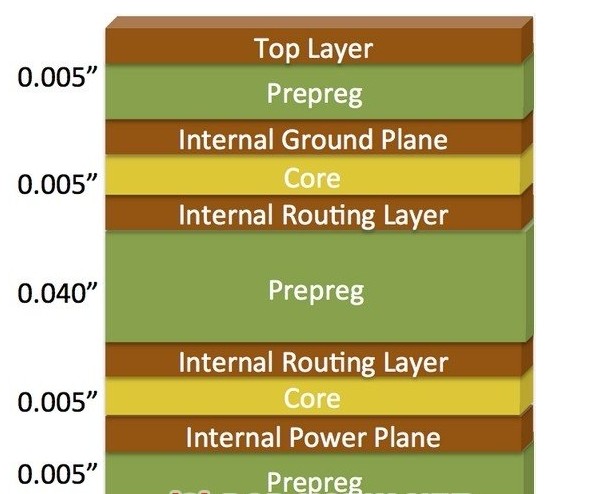
Hereby we would like to take an example of a 4 layer circuit board will be described to explain how the arrangement and combination of various Standard Multilayer Circuit Board Stackup Structure are preferred.
For the commonly used 4-layer boards, there are several stacking methods (from top to bottom).
(1) Siganl_1 (Top), GND (Inner_1), POWER (Inner_2), Siganl_2 (Bottom).
(2) Siganl_1 (Top), POWER (Inner_1), GND (Inner_2), Siganl_2 (Bottom).
(3) POWER (Top), Siganl_1 (Inner_1), GND (Inner_2), Siganl_2 (Bottom).

Obviously, the lack of effective coupling between the power layer and the ground plane of scheme 3 should not be adopted.
So how should Option 1 and Option 2 be chosen? In general, the designer will choose option 1 as the structure of the 4-layer board. The reason for the selection is not that Option 2 cannot be used, but that the general PCB board only places components on the top layer, so it is more appropriate to adopt Option 1.
However, when components need to be placed on the top and bottom layers, and the thickness of the medium between the internal power layer and the ground layer is large which will result in bad quality of the coupling, it is necessary to consider which layer has fewer signal lines. For scheme 1, the bottom layer has fewer signal lines, and a large-area copper film can be used to couple with the POWER layer. Conversely, if the components are mainly disposed on the bottom layer, scheme 2 should be used to manufacture printed circuit board.

internal power layer and the ground layer
If the laminated structure shown in Figure 11-1 is used, the power supply layer and the ground layer itself are already coupled. Considering the requirement of symmetry, Scheme 1 is generally adopted.
After the analysis of the laminated structure of the 4-layer board is completed, the arrangement and combination method of the 6-layer board laminated structure and the preferred method will be described below by way of an example of a 6-layer board combination.
(1) Siganl_1 (Top), GND (Inner_1), Siganl_2 (Inner_2), Siganl_3 (Inner_3), POWER (Inner_4), Siganl_4 (Bottom).
Scheme 1 uses four layers of signal layers and two layers of internal power/ground layers. It has more signal layers, which is beneficial to the wiring work between components. However, the defects of this scheme are also obvious, which are manifested in the following two aspects.
1 The power and ground planes are separated far apart and are not fully coupled.
2 The signal layer Siganl_2 (Inner_2) and Siganl_3 (Inner_3) are directly adjacent, and the signal isolation is not good, and crosstalk is easy to occur.
(2) Siganl_1 (Top), Siganl_2 (Inner_1), POWER (Inner_2), GND (Inner_3), Siganl_3 (Inner_4), Siganl_4 (Bottom).
Compared with scheme 1, scheme 2 has sufficient coupling between power layer and ground plane, which has certain advantages over scheme 1, but Siganl_1 (Top) and Siganl_2 (Inner_1) and Siganl_3 (Inner_4) and Siganl_4 (Bottom) signal layers are directly Adjacent, the signal isolation is not good, and the problem of crosstalk is not solved.
(3) Siganl_1 (Top), GND (Inner_1), Siganl_2 (Inner_2), POWER (Inner_3), GND (Inner_4), Siganl_3 (Bottom).
Compared with schemes 1 and 2, scheme 3 reduces one signal layer and adds one inner layer. Although the available wiring level is reduced, the solution solves the defects common to schemes 1 and 2.


