Soldering Integrated Circuit Ground Pin in PCB Reverse Engineering
All soldering integrated circuit ground pin in PCB Reverse Engineering should be soldered directly to the low impedance ground plane to minimize series inductance and resistance. The use of traditional IC sockets is not recommended with high speed devices. The extra inductance and capacitance of even “low profile” sockets may corrupt the device performance by introducing unwanted shared paths.
If sockets must be used with DIP packages, as in prototyping, individual “pin sockets” or “cage jacks” may be acceptable. Both capped and uncapped versions of these pin sockets are available (AMP part numbers 5-330808-3, and 5-330808-6). They have spring-loaded gold contacts which make good electrical and mechanical connection to the IC pins. Multiple insertions, however, may degrade their performance.
Power supply pins should be decoupled directly to the ground plane using low inductance ceramic surface mount capacitors. If through hole mounted ceramic capacitors must be used, their leads should be less than 1 mm. The ceramic capacitors should be located as close as possible to the IC power pins. Ferrite beads may also be required for additional decoupling.
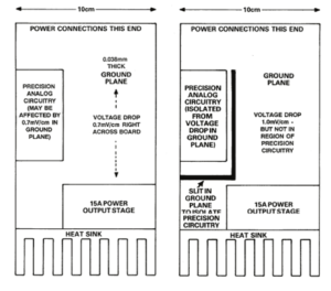
So, the more ground the better—right? Ground planes solve many ground impedance problems, but not all. Even a continuous sheet of copper foil has residual resistance and inductance, and in some circumstances, they can be enough to prevent proper circuit function. Below Figure shows such a problem—and a possible solution.

A Slit in the Ground Plane Can Reconfigure Current Flow for Better Accuracy


