Smaller Package in PCB Board Layout
Modern assembly practices have favored Smaller Package in PCB Board Layout such as eight pin MINI-DIP and SOIC types. Some suggested partial layouts for guard circuits using these packages are shown in the next two figures. While guard traces may also be possible with even more tiny op amp footprints, such as SOT-23 etc., the required trace separations become even more confining, challenging the layout designer as well as the manufacturing processes.
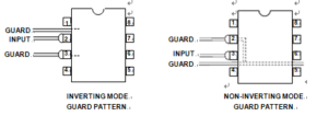
For the ADI “N” style MINI-DIP package, Below Figure illustrates how guarding can be accomplished for inverting (left) and non-inverting (right) operating modes. This setup would also be applicable to other op amp devices where relatively high voltages occur at pin 1 or 4. Using a standard eight pin DIP outline, it can be noted that this package’s 0.1″ pin spacing allows a PC trace (here, the guard trace) to pass between adjacent pins.

PCB Guard Patterns for Inverting and Noninverting Mode Op Amps Using Eight Pin MINI-DIP (N) Package
This is the key to implementing effective DIP package guarding, as it can adequately prevent a leakage path from the –VS supply at pin 4, or from similar high potentials at pin 1.


