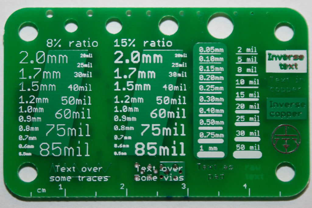
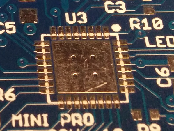
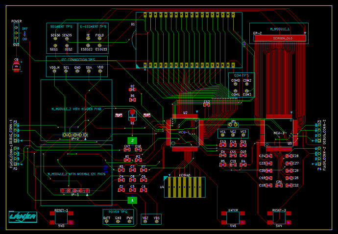
PCB Board Cloning Process is always related to record the information of components solder on the original PCB board, and then make a 100% perfect clone we can print the same silkscreen notification on the newly made PCB board. but sometimes the original PCB board doesn’t come with the silkscreen on it, in this case we have compiled the information by engineer and print it onto it when clone PCB board, hereby let’s talk about the silkscreen specification:

All components, mounting holes and positioning holes have corresponding silkscreen labels. In order to facilitate the installation of the circuit boards, all components, mounting holes and positioning holes have corresponding silkscreen labels. The mounting holes on the PCB are printed with H1. H2…Hn is identified.
The silk screen characters follow the principle of left-to-right and bottom-up and it should also follow the principle of left-to-right and bottom-up as much as possible. For components with polar electrodes such as electrolytic capacitors and diodes, try to keep them in each functional unit. The direction is the same.
There is no silkscreen on the device pad and the tin ball that needs tin-plugging. The device bit number should not be blocked by the device after installation. (Higher density, except for silkscreen on the PCB).
In order to ensure the soldering reliability of the PCB, there is no silk screen on the device pad; in order to ensure the continuity of the tin solder, it is required to have no silkscreen on the tin ball; in order to facilitate the PCB Board insertion and maintenance, the device bit number should not be After installation, the device is blocked; the silk screen cannot be pressed on the via holes and the pads to avoid partial silk screen loss when the solder mask is opened, which affects the identification. Screen printing spacing is greater than 5 mils.

The polarity of the polar components is clearly indicated on the silk screen, and the polarity direction marks are easy to identify.
Directional connectors whose orientation is clearly indicated on the silk screen.
There should be a bar code position mark on the PCB. When the PCB board space is allowed, there should be a 42*6mm bar code screen frame on the PCB. The position of the bar code should be convenient for scanning.
PCB board name, date, version number, etc. The position of the board information silk screen should be clear. The PCB file should have the board name, date, version number, etc., and the board information silk screen, the position is clear and eye-catching.

PCB should have complete information about the PCB manufacturer and anti-static mark.
The number of sheets in the PCB illuminating file is correct. Each layer should have the correct output and have a complete layer output.
The identifier of the device on the PCB must match the identifier in the BOM list.


