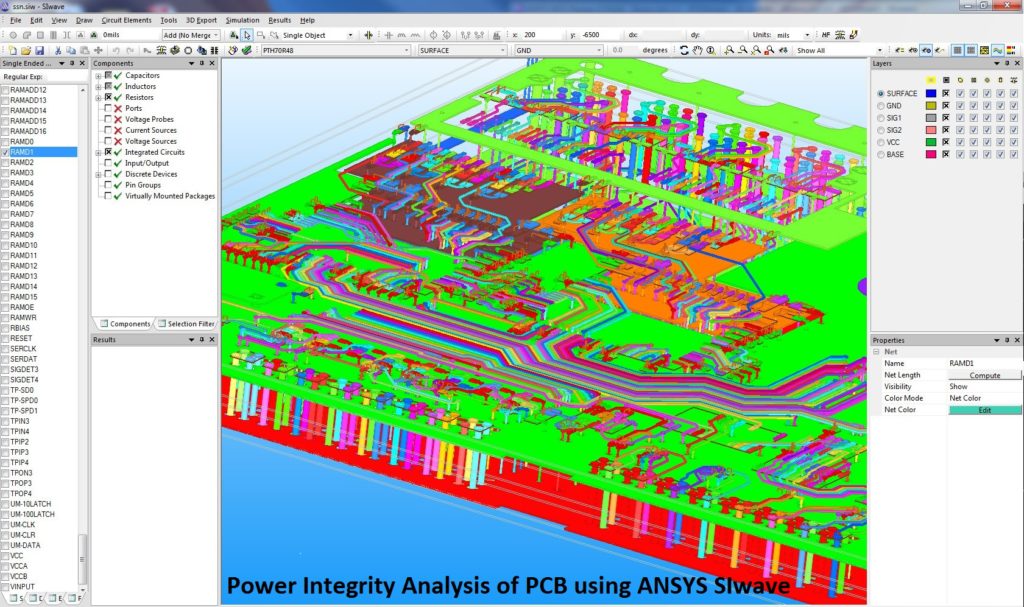
Signal Integrity of PCB Circuit Board Cloning is the ability of a signal to respond in the PCB circuit board with the correct timing and voltage. If the signal in the PCB circuit board can reach the IC with the required timing, duration, and voltage amplitude, the circuit has better signal integrity. Conversely, when the signal does not respond properly, a signal integrity problem occurs. Broadly speaking, signal integrity problems are mainly manifested in five aspects: delay, reflection, crosstalk, synchronous switching noise (SSN) and electromagnetic compatibility (EMI) as well as ESD SUPPRESSION ON ELECTRONIC BOARD CLONING.
Delay means that the signal is transmitted at a limited speed on the circuitry wire of the PCB circuit board, and the signal is sent from the transmitting end to the receiving end with a transmission delay. The delay of the signal affects the timing of the system. In high-speed digital systems, the propagation delay depends primarily on the length of the wire and the dielectric constant of the medium surrounding the wire.

In addition, when the characteristic impedance of the wire on the PCB (called the transmission line in the high-speed digital system) does not match the load impedance, a part of the energy will be reflected back along the transmission line after the signal reaches the receiving end, causing the signal waveform to be distorted or even appearing. Overshoot and undershoot. If the signal is reflected back and forth on the transmission line, ringing and surround oscillations will occur and causing problem on Signal Integrity of PCB Circuit Board Cloning.
Since there is mutual capacitance and mutual inductance between any two devices or wires on the PCB, when the signal on one device or one wire changes, the change will affect other devices through mutual capacitance and mutual inductance. Wire, which is crosstalk. The strength of the crosstalk depends on the geometry and mutual distance of the device and the wires which can affect the Signal Integrity of PCB Board Cloning.
When many digital signals from the PCB circuit board cloning are switched synchronously (such as the CPU’s data bus, address bus, etc.), due to the impedance on the power and ground lines, synchronous switching noise will occur, and ground level bounce will occur on the ground. Noise (referred to as ground bounce). The strength of the SSN and ground bounce also depends on the IO characteristics of the integrated circuit, the impedance from REVERSE ENGINEERING CIRCUIT CARD POWER & GROUND, and the layout and routing of high speed devices on the PCB circuit board.
In addition, like other electronic devices, PCBs also have electromagnetic compatibility problems, and their generation is mainly related to the layout and wiring of PCB boards.


