Generally speaking, Reverse Engineering Printed Circuit Board is get the target board scanned and recording the position of each one of the component in detail, then de-soldering components off PCB to make a bill of materials (BOM) and the material procurement.

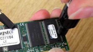
desolder pcb part
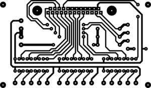
The empty board will be scanned into a high resolution picture and processing by the image editing software such as Photoshop, and then use PCB design application to restore Printed circuit board layout drawing from the scanning pictures, and then the PCB layout drawing will be sent to manufacturer. After the board is made, the purchased components are soldered to the blank PCB board, and then the circuit board is tested and debugged.

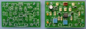
PCB after desolder its component
The specific technical steps are as follows:
The first step is to get a physical target PCB. Record the model number, parameters, and position of all components on the paper, especially the direction of the diode, the transistor, and the orientation of the Integrated circuits. It is best to take photos of component locations.
In the second step, de-solder all components and remove the tin residue from the PADs’ hole. Clean the PCB with alcohol and placed in the scanner. The scanner needs to increase the scanned pixels slightly in order to get a clearer image. The top layer and the bottom layer were then slightly polished with water-based tissue paper, polished until the copper film is shiny, then place it in the scanner, and activate the PHOTOSHOP. The two layers were separately scanned in different colors. Note that the PCB must be placed in the scanner properly. Otherwise, the scanned image cannot be used.

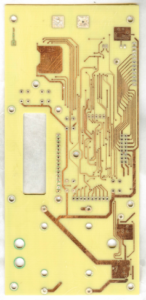
PCB after strip off the solder resist
The third step is to adjust the contrast, lightness and darkness of the canvas so that the part with the copper film and the part without the copper film are strongly contrasted. Then turn the sub-graph into black and white. Check if the lines are clear. If not, repeat this step. If it is clear, save the picture as black and white BMP format files, name as TOP.BMP and BOT.BMP. If you find any problems with the graphics, you can use PHOTOSHOP to repair and rectify them.
The fourth step, the two BMP format files are converted to PROTEL format files, transferred to two layers in PROTEL, if the PADs and VIAs on two layers can overlay each other properly, indicating we have done a good job from previous steps, if there is a deviation, repeat the third step. Therefore, Reverse Engineering Printed Circuit Board is a job that needs a lot of patience, because a small problem or deviation will affect the quality and the degree of matching.
The fifth step is to convert the BMP of the TOP layer to TOP.PCB. Note that the layer to be converted into the SILK layer is the yellow layer. Then you trace the line at the TOP layer and place the components according to the drawing made from the second step. After drawing has been made completely, delete the SILK layer. Repeat until you have drawn all the layers circuitry pattern.
In the sixth step, the TOP.PCB and BOT.PCB will be transferred into PROTEL, and integrate into a single diagram. use a laser printer to print TOP LAYER and BOTTOM LAYER respectively on the transparent film (1:1 ratio), put the film on the PCB, and compare if there is something wrong.
Now, a complete Printed circuit board reverse engineering process has been done, but it was only half completed. Tests are also conducted to check whether the electronic circuitry pattern is 100% the same as the original board.


