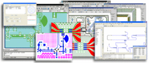
Reverse Engineering Printed Circuit Board Design Process will introduce how to reverse engineering pcb board hardware through delayering the copper circuitry to make diagram and restore schematic from circuit board netlist and layout file;

Reverse Engineering Printed Circuit Board Design Process will introduce how to reverse engineering pcb board hardware through delayering the copper circuitry to make diagram and restore schematic from circuit board netlist and layout file
When hardware project personnel need to conduct PCB layout drawing redesign, they must submit a PCB board investment application in the “PCB Design Investment Application Form”, and after approval by their project manager and planning office, the process status reaches the designated PCB design department for approval.
Project personnel must prepare the following information: After review, completely correct schematic diagrams restoration, including paper documents and electronic files; Formal BOM with MRPII component code;
The PCB structure drawing should indicate the dimensions, the size of the mounting holes and the positioning dimensions, the positioning dimensions of the connectors, and the prohibited wiring area;

For new devices, that is, devices without MRPII codes, packaging materials are required; The above information is approved by the designated PCB design department and the PCB designer is designated before the PCB circuit board gerber file redrawing can be started.


