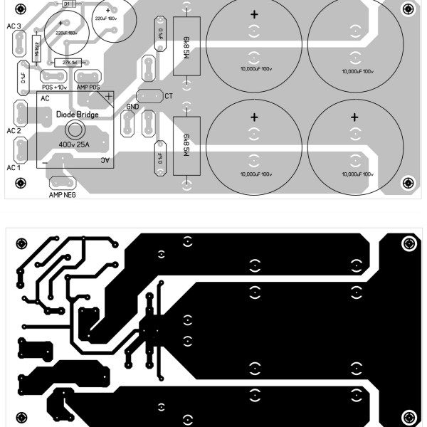
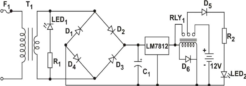
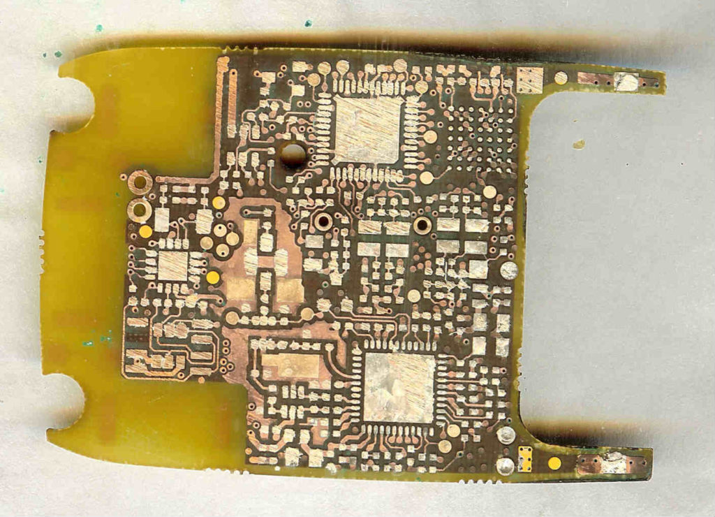
Power Supply PCB Board has been commonly used in the electronic device, as a result of that, a good layout will help to provide high efficient energy to the whole system, unfortunately not all of the power supply board is capable of it, so it is necessary to Reverse Engineering Power Supply PCB Board layout and then redesign the Board Layout to optimize it, hereby we would like to introduce some of the layout skill, see below:
First of all, The input and output terminals of the power filter should be kept away from each other during layout to avoid noise coupling from the input to the output.
Secondly, Whether it is a differential mode filter circuit or a common mode filter circuit, the leads on the capacitor and the inductor should be widened as much as possible;

3rd, The decoupling tantalum capacitor of the power supply should be close to the output position of the voltage regulation module. The filter tantalum capacitor voltage in the power supply circuit should be designed with 1/3 derating.
4th Under the premise of satisfying the PCB board thermal design, the power supply part layout should be compact, the compact layout can reduce the length of the connection, reduce the adverse effects caused by the distributed parameters on the connection line, and the compact layout can reduce the power supply loop area.
5th The input and output filter layout of the power supply is as close as possible to the power inlet;
6th The power supply part should be layout according to the flow direction of the power supply current. The power input and output should be separated, and the power supply layout should be designed in a straight line. Try not to use the bypass layout to prevent the power supply from interfering with each other.

7th The layout of the power supply section should be kept away from unrelated strong interference circuits and devices as much as possible to prevent external noise from being coupled into the power supply and causing power fluctuations.
8th The power supply layout is conducive to the formation of small power supply loops to reduce the external interference of these loops, and these small loops can also reduce the interference of external noise on the power supply.
9th The layout of the power supply should be as close as possible to the powered device to shorten the power transmission path and reduce the adverse effects of distributed parameters on the power transmission path.

10th Powering the LDO as close as possible to the powered device, pay special attention to those LDOs that output low voltage;


