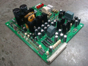
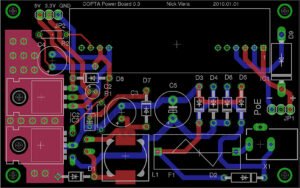
Reverse Engineering Power Supply PC Board can help engineer to extract layout drawing, gerber file, BOM List and schematic diagram from original Power supply printed circuit board, the procedures as below:
First: Accept the power supply PC board layout redesign requirements! Evaluate the cost and make a feasible plan.
Secondly: According to the customer’s quotation! Given the general component cost and production cost, a feasible circuit diagram reverse engineering.

Reverse Engineering Power Supply PC Board can help engineer to extract layout drawing, gerber file, BOM List and schematic diagram from original Power supply printed circuit board
Thirdly: Restoring a PCB board schematic diagram! Determine the selected power tube, transformer, the most stable, simplest production and convenient principle scheme.
Four: Redesign the PCB according to the schematic diagram, the sample requirements or the enclosure requirements given by the customer.
Fifth: According to the schematic diagram, assemble suitable components and adjust the electrical parameters. Let this power supply pc board work normally under the minimum requirements.
Sixth: Load test, power up to 80 test type, check output waveform, voltage requirements, electromagnetic performance, power tube temperature, voltage stability, conversion efficiency. In this process, appropriate parameter adjustments are made to the electronic components.
Seventh: Strengthen the test! That is, tests such as super negative, short circuit, low voltage, over voltage, strong temperature, shock resistance, etc.

Redesign the PCB according to the schematic diagram, the sample requirements or the enclosure requirements given by the customer
Eighth: Determine the accurate parameters of the schematic diagram according to the template, determine the orientation diagram, material diagram, and send it to the production department, warehouse manager, and merchandiser to produce small batches of the template.
Ninth: Perform rigorous testing on the model, and the various performances are OK, and the salesman will send it to the customer for evaluation. OK, ready for mass production.
Tenth: Follow up and improve the project in the future production, and ship to customers in the shortest time and with the best quality.


