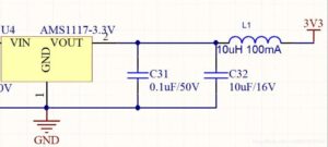
Reverse Engineering PCB Board Schematic Drawing which can be used to repair mal-functional electronic circuit board, schematic diagram itself must increase its maintainability, see below image:

Reverse Engineering PCB Board Schematic Drawing which can be used to repair mal-functional electronic circuit board
Increase the L1 inductance in the new PCB board schematic diagram after reverse engineering so that it can be disconnected during maintenance, making it easier to troubleshoot.
Inductance, magnetic beads or 0R resistors can be used here, depending on the specific situation. However, there are special circumstances. If the load is extremely large, the power of the serial-in components required is large, and the cost increase is too much, and it is not worthwhile.
At this time, it is not necessary to add it. If a chip such as a QFP-64 package is followed, and the power is relatively small, components can be connected in series, because there will be more cases of poor QFP soldering.

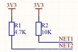
The BOM List is the bill of materials. Try to keep the types of materials as few as possible, so that the buyer can reduce the workload, and it will also reduce many problems in the electronic PCB card re-manufacturing. There are two pull-up resistors, one 4.7K and one 10K. If this resistance has little effect, you can combine them into 10K. The decoupling capacitor is also the same operation, we must draw inferences about it.


