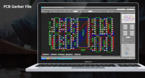
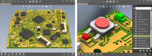
Reverse Engineering PCB Board Schematic Diagram starts from de-solder all the parts off the PCB board, we should firstly carve out different zones according to functions: During the process of PCB layout diagram recreating, carve up different zones according to module function can greatly help engineers to avoid some unnecessary troubles, improve efficiency of drawing. Generally speaking, the components of Printed Circuits Boards which work for same functions can be centralized, which can bring more convenience evidence for extract circuit board’s schematic diagram.

Reverse Engineering PCB Board Schematic Diagram
However, Carve up functional module isn’t at random. It requires engineers to have better knowledge of electronic and electric on the electronic printed circuit board. First of all, find out the core part of the single functional unit, and then through this core part can find out other components, finally form a function subarea. Establishment of function subarea is the basement of compile circuit board’s schematic diagram. Additional, during this process, those designators of components in sequence can also help you locate the function subarea sooner.

according to these standard part’s lead can to great extend ensure the accuracy of schematic diagram extraction from PCB Reverse Engineering
The subsequent process is orient the right part, the so call right part as a standard one can be viewed as the main part before the PCB schematic diagram being extracted from circuit board, according to these standard part’s lead can to great extend ensure the accuracy of schematic diagram extraction from PCB Reverse Engineering.
In view of engineer, it isn’t too much trouble for them to locate standard part, generally, they can choose those parts which play the main role in the functional module, they usually have more leads and bigger size which could be helpful for drawing, such as integrate circuit, transformer and crystal.


