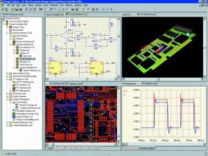
Reverse Engineering PCB Board Design Process refers to the process that the designer collects and processes the surface and interior of the electronic circuit board with components, and converts the image file into a circuitry layout pattern file through the reverse engineering PCB board software, and through the printed circuit board manufacturing software, manufacturing processing, etc.

Reverse Engineering PCB Board Design Process refers to the process that the designer collects and processes the surface and interior of the electronic circuit board with components, and converts the image file into a circuitry layout pattern file
The Reverse Engineering electronic circuit Board Design Process is:
product sample → data collection → data processing → cloning PCB board → PCB layout to schematic diagram → new product.
In these aspects of reverse design, data collection, data processing, cloning circuit board, and PCB layout to schematic diagram are the four key links in reverse engineering circuit board design of product design.


