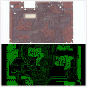
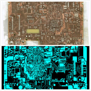
Reverse Engineering PCB Board Design File follows the blueprint established by the PCB board schematic diagram flow, but, as mentioned before, these two files are very different in appearance.
We have discussed PCB schematics, but what differences can be observed in the design files? When we talk about PCB design files, we are talking about a 3D model, which includes a printed circuit board and design files. They can be single layer or multiple layers Printed circuit board, although two layers are most common.

Reverse Engineering PCB Board Design File follows the blueprint established by the PCB board schematic diagram flow, but, as mentioned before, these two files are very different in appearance.
We can observe some differences between PCB schematics and PCB design files: All components are sized and positioned correctly If two points should not be connected, they must go around or switch to another PCB layer to avoid crossing each other on the same layer In addition, as we briefly talked about, reverse engineering PCB card design pays more attention to actual performance, because this is to some extent the verification phase of the final product.
At this point, the practicality of the design must actually work comes into play, and the physical requirements of the printed circuit board file cloning must be considered. Some of these include: How does the spacing of the components allow sufficient heat distribution

At this point, the practicality of the design must actually work comes into play, and the physical requirements of the printed circuit board file cloning must be considered. Some of these include: How does the spacing of the components allow sufficient heat distribution
Connectors at the edge Regarding current and heat issues, how thick the various traces must be Because physical limitations and requirements mean that PCB design files cloning usually look very different from the design on the schematic, the design files include a silk screen layer. The silk screen layer indicates letters, numbers and symbols to help engineers assemble and use the board. It is required to work as planned after all components are assembled on the printed circuit board. If not, you need to redraw.


