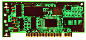
Reverse Engineering PCB Board Anti-Interference Layout Diagram, generally speaking, should conform to the principles of electrical interference and easy heat dissipation between the devices, and this process can help to extract the circuit diagram from original PCB board when the absence of necessary documents to make improvement of circuit board original layout diagram, there are power transformers, analog devices, digital devices, digital logic devices, output drive devices, etc.

① Use high-power and strong electric devices such as power transformers and output drive devices as a
centralized layout of printed circuit board:
② Use digital logic devices as a type of centralized arrangement;
③ Assemble the susceptible analog devices as a type of printed circuit board centralized layout. For example, the clock input of the clock generator and the crystal XPU are prone to noise, and they should be placed closer when arrange the components of PCB board layout drawing. For those devices that are prone to noise small current circuit, high current circuit, switch circuit, etc.
It should be kept away from the logic control circuit and storage circuit of the micro-controller as much as possible. These circuits can be made into circuit boards separately, which is beneficial to anti-interference and improves the reliability of the circuitry system, In addition, each type of device according to the principle of electrical anti-interference, it is further classified and arranged.


