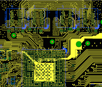
PCB Board Layout plays a key role in high-speed circuits, but it is often one of the last steps in the Reverse Engineering High Speed PCB Board layout process. There are many problems with high-speed PCB board layout, through reverse engineering technique we can improve the performance;
This paper mainly discusses the layouting problem of high-speed PCB Boards from the perspective of practice. The main purpose is to help new users pay attention to the many different issues that need to be considered when re-design high-speed PCB board layout. Another goal is to provide a review for customers who have not been exposed to PCB Layout for some time. and it is impossible to discuss all the issues in detail, but we will discuss the key parts that have the greatest impact on improving printed circuit board performance, shortening design time, and saving modification time through PCB reverse engineering.

Although primarily directed to circuits associated with high speed operational amplifiers, the problems and methods discussed herein are generally applicable to wiring for most other high speed analog circuits. When an op amp is operating in a very high radio frequency (RF) band, the performance of the circuit is highly dependent on the PCB board layout. The high-performance circuit design that looks good on the “drawings”, if it is affected by the carelessness of the layout, can only get ordinary performance.

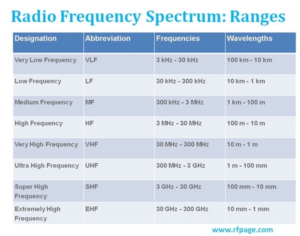
high radio frequency (RF) band
Pre-considering and paying attention to important details throughout the Layouting process will help ensure the desired circuit performance and normally through reverse engineering to obtain the schematic diagram of PCB board will help to improve the performance even if the first version is not very well resulted.


