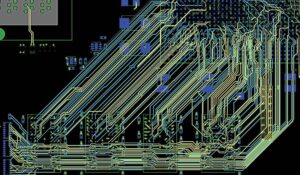
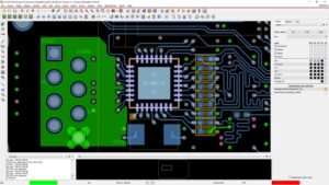
Reverse Engineering High Speed Circuit Board Schematic Diagram to avoid circuitry pattern layout at 90° corners, High-frequency and high-speed signal transmission lines should avoid routing at 90° corners, which is strongly required in various PCB Design Guides and rule checking.

Reverse Engineering High Speed Circuit Board Schematic Diagram
Because when clone high-frequency and high-speed signal transmission PCB board lines need to maintain the same characteristic impedance, use 90° corner routing and place them at the corners of the transmission line, Will change the line width, the line width at the 90° corner is about 1.414 times the normal line width. Because the line width is changed, it will cause signal reflection.
At the same time, the extra parasitic capacitance at the corner will also cause time for signal transmission and delay the impact. Of course, when the signal propagates along the uniform interconnection line, there will be no reflection and distortion of the transmission signal.

Because when clone high-frequency and high-speed signal transmission PCB board lines need to maintain the same characteristic impedance, use 90° corner routing and place them at the corners of the transmission line,
If there is a 90° corner on the uniform interconnection line, the PCB transmission line width will change at the corner. According to the relevant calculation of electromagnetic theory, this will definitely bring about the reflection effect of the signal. This is the case in theory, but the theory is the theory after all. Does the actual situation have a significant impact on high-speed signal transmission lines?
Therefore, a 90° corner will have a negative impact on high-speed signal transmission lines, which is theoretically certain, but is this impact fatal? Does the 90° corner have the same effect on high-speed digital signals and high-frequency microwave signal transmission lines?


