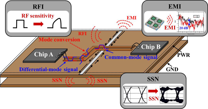
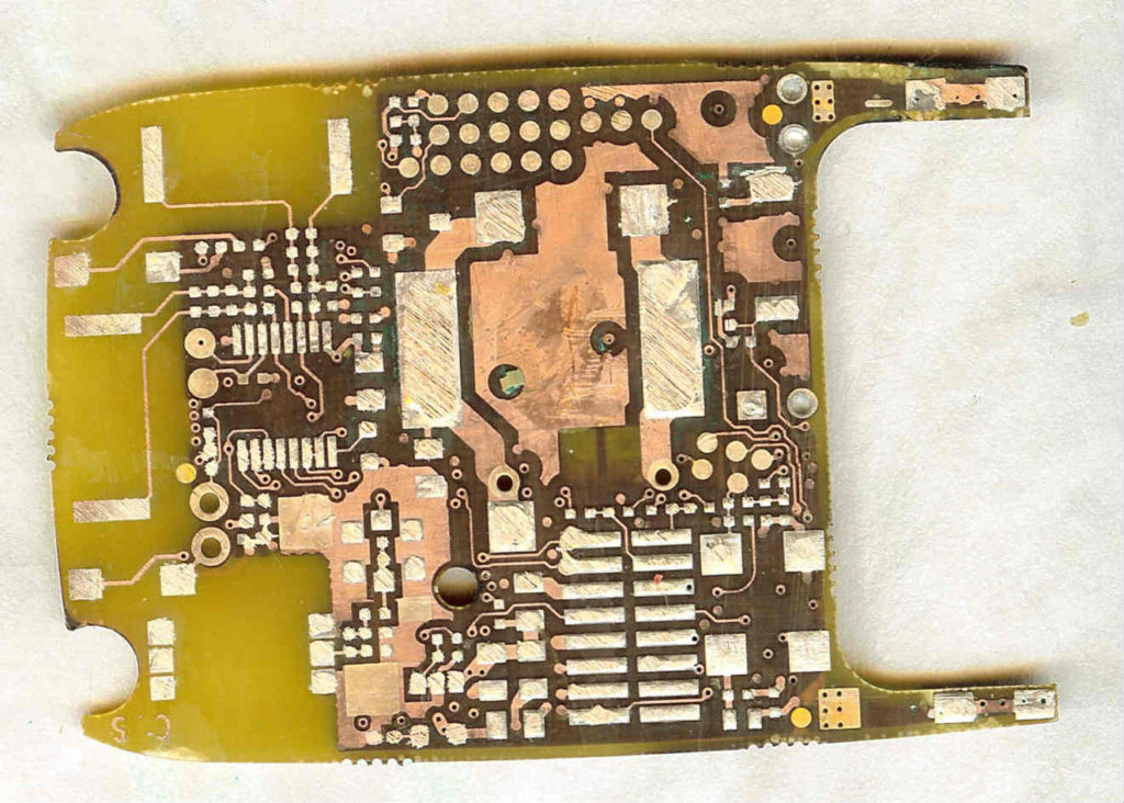
Reverse Engineering Circuit Board to Reduce Noise & Electromagnetic Inteference can be carried out through below practical aspects:

The printed circuit board is divided by frequency and current switching characteristics, and the noise component is farther away from the non-noise component.
Single-panel and dual-panel single-point power supply and single-point grounding, power supply track, and grounding wire are as thick as possible. If the economy is affordable, use a multi-layer board to reduce the capacitive inductance of the power supply ground.
Keep clock, bus, and chip select signals away from I/O lines and connectors.
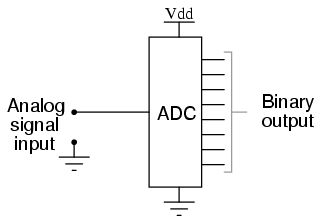
The analog voltage input track and reference voltage terminal should be as far as possible from the digital circuit signal line, especially the clock.

analog voltage input track
For A/D type devices, the digital part and the analog part are more uniform and do not cross.
The clock line is perpendicular to the I/O line and has less interference than the parallel I/O line, and the clock component pins are far from the I/O cable.
The component pins are as short as possible and the decoupling capacitor pins are as short as possible.
The key lines should be as thick as possible and with protective ground on both sides. The high speed line should be short and straight.

Noise sensitive lines should not be parallel to high current, high speed switching lines.
Do not route underneath the quartz crystal and below the noise sensitive device.
For weak signal circuits, do not form a current loop around the low frequency circuit.
Do not form a loop in the signal. If it is unavoidable, make the loop area as small as possible.
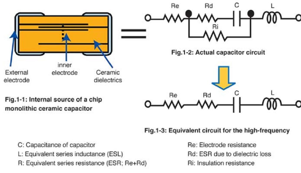
One decoupling capacitor per integrated circuit. A small high frequency bypass capacitor is added to each electrolytic capacitor.

high frequency bypass capacitor
Use a large-capacity tantalum capacitor or a condenser capacitor instead of an electrolytic capacitor for the circuit to charge and discharge the storage capacitor. When using a tubular capacitor, the housing should be grounded.


