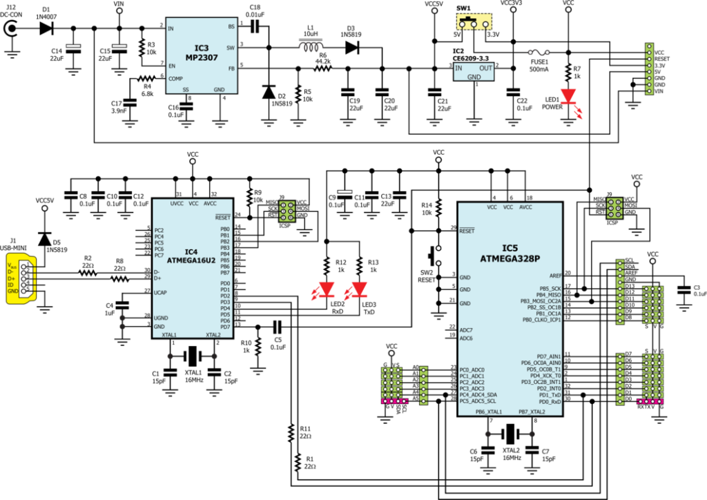
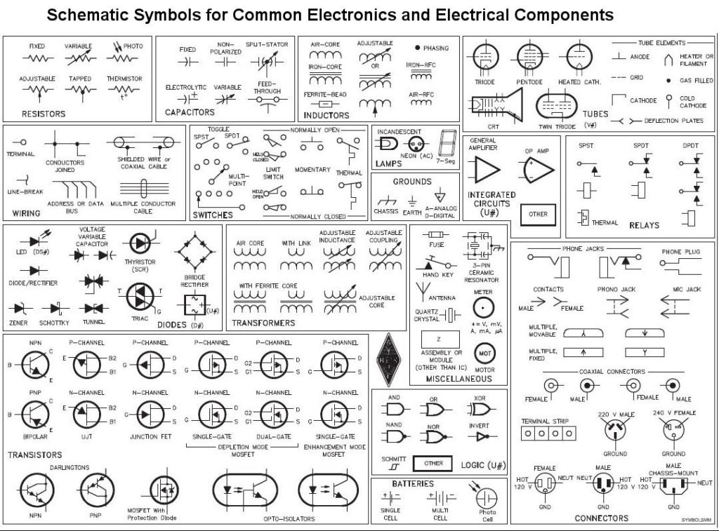
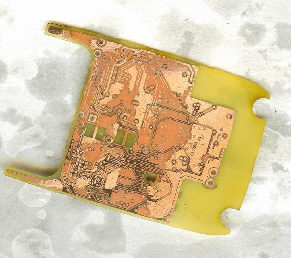
When we get the circuit board, we must first read the schematic diagram. After understanding the schematic diagram, we can start to reverse engineering circuit board. The main idea of circuit board schematic diagram reverse engineering should be according to the signal flow direction, so that the flow of the signal is as smooth as possible. As far as possible, the loop will not wrap around.

Generally, the interface device can be layout first, then the interface protection device, then the main power module, then the layout of the function module connected to the interface, and then the layout of the main component module, such as CPU, DDR, main Large functional modules, after placing these components footprint, layout the remaining devices, such as small LDO power supplies, indicator lights, buffers, crystals, etc. The techniques for Reverse Engineering Circuit Board’s key signals or modules are described below.

Below refers to the interface circuit device layout skills:
- The filter components of the interface circuit need to be arranged according to the flow direction of the signal. The filtered output should be as far as possible from the input, so as to prevent the input signal from being coupled into the output signal.
- Isolation performance of the isolation transformer shouldn’t be damaged during layout. The primary and secondary coil pins of the isolation transformer must be placed on the protection ground and the working ground.
- Common mode inductors for external interface circuits such as Ethernet ports, telephone network ports, and USB ports. The magnetic beads should be placed on the boundary between the working ground and the protective ground. The dividing boundary between the protective ground and the working ground should be as close as possible to the external interface connector;
- Some devices and circuits with relatively large noise in ordinary digital circuits (such as crystal oscillators, clock drivers, high-speed processors, some high-speed digital circuits, etc.) should be placed as far as possible from external interface circuits.
- The layout of the interface device is arranged in a line arrangement. The surge protection device is placed first, and then the filter device is placed to avoid coupling between the signal lines before and after the signal line is routed.
- Some common mode inductors for suppressing common mode noise added to the external interface circuit such as network port and USB port should be placed as close as possible to the port during layout to reduce the noise radiated inside the board and reduce external noise coupling. Come in.
- For products with external power adapter, the magnetic beads and inductors on the DC power input port power supply and ground signal should be placed as close as possible.
- The layout between the ports should not be interlaced as much as possible to prevent the ports from interfering with each other.


