Reverse Engineering Circuit Board preparation
The first step of Reverse Engineering Circuit Board preparation:
Get a good circuit board, to see if there is any component with extra height, if yes, then we have to record component number, component package, temperature value, etc in detailed documentation.
Before remove the components from circuit board, it is better to scan them as a backup. After removing those height components, the SMD and some smaller components are left.

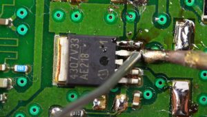
desolder part off the pcb
At this time, the second scan is performed to record the image. The recommended resolution is 600 dpi. Be sure to remove dirt from the PCB surface before scanning to ensure that the scanned IC model and the characters on the PCB are clearly visible on the image.
Step 2: Components De-soldering and Compiling BOM
Use a small air gun to heat the components mounted on the circuit board which is going to be reverse engineered, and then use tweezers to hold the components to prevent it has been blow away by the hot wind, and take it off from circuit board soldering pads.
The de-soldering process will be executed in order, start from the resistor, then capacitor, and finally remove the IC. Record the presence or absence of components that have been dropped and previously installed. Before de-soldering, prepare a form with a record of the item number, package, model number, value, etc., and stick the double-sided tape on the component record form.

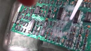
clean pcb residue on the surface after desoldering
After the lower number, the removed components are affixed one by one to the position corresponding to the designator of position number.

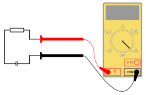
measuring resistor on the pcbgif
After de-soldering all the components, the value of these components are measured by electrical bridge (some devices will change their own values under the action of high temperature, so they should be measured after the temperature decreased to the normal level, measurements are taken and the measured value is more accurate. After the measurement is completed, the data has to be stored into the computer for archiving.


