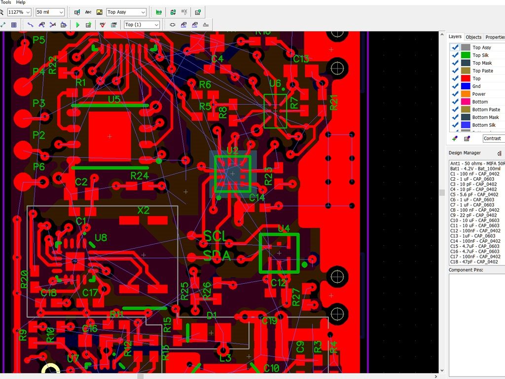
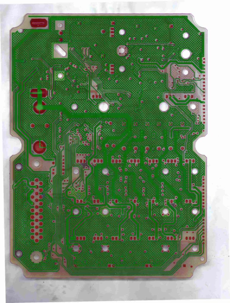
Reverse Engineering Circuit Board Layout Scheme can choose whether the target is double-sided boards or multi-layer boards and it depends on the highest operating frequency and the complexity of the circuit system, as well as the requirements for assembly density.

When the clock frequency exceeds 200 MHz, the multi-layer PCB board circuitry drawing copy is required to fufill the task. If the operating frequency exceeds 3 500 MHz, it is best to choose PTFE as the dielectric layer of the printed circuit board raw material, because of its high frequency attenuation, low parasitic capacitance, fast transmission speed, and low power consumption.
The principles of Reverse Engineering PC Board Layout are as follows:
A • The printed conductors should be as short as possible, especially in high-frequency loops. The corners of the conductors should be rounded or 45 ° when turning, to avoid sharp or right angles.

Because the right-angle traces easily lead to resistance to abrupt changes, leading to signal emission, which can cause oscillation or overshoot, forming strong radiation. The right angle or the sharp angle not only affects the electrical performance in the case of high-frequency circuits and high wiring density, but also the corrosion agent is more likely to remain in the included angle during the production process, resulting in excessive etching.
B • Width of wire
The featured characteristic impedance of the microstrip line on the printed circuit board reverse engineering is generally between 50 and 1 20mil. To achieve a large characteristic impedance, the line width must be made very fine. But very thin wires are not easy to make. Taking into account various factors, generally choose the right and left impedance value ratio is appropriate, because the selected characteristic impedance can achieve the best balance between delay time and power consumption.


