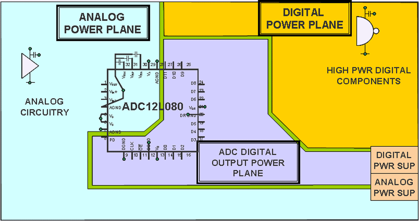
Reverse Engineering Amplifier Mixed Signal PCB Board Layout Design can use partition design method to reduce the mutual interference between digital and analog signals; Before redesigning PCB board layout for better emc performance, we must understand the two basic principles of electromagnetic compatibility (EMC):

Reverse Engineering Amplifier Mixed Signal PCB Board Layout Design can use partition design method to reduce the mutual interference between digital and analog signals
The first principle is to minimize the area of the current loop;
The second principle is that the system uses only one reference surface. On the contrary, if there are two reference planes in the system, it is possible to form a dipole antenna (Note: The radiation size of a small dipole antenna is proportional to the length of the line, the amount of current flowing and the frequency);
If the signal cannot return through the smallest possible loop, it may form a large loop antenna (Note: the radiation size of a small loop antenna is proportional to the loop area, the current flowing through the loop, and the square of the frequency ). Avoid these two situations as much as possible in the design.
It was suggested that the digital and analog circuit card grounds on the mixed-signal circuit board reverse engineered layout design be separated to achieve isolation between the digital and analog grounds.
Although this method is feasible, there are many potential problems, especially in complex large-scale systems. The most critical issue is that the wiring cannot be crossed across the division gap. Once the wiring across the division gap is crossed, the electromagnetic radiation and signal crosstalk will increase dramatically.
The most common problem in PCB design is that the signal line crosses the divided ground or power supply and generates EMI problems.


