Reverse Engineering A PCB Board to Avoid Sharp Angle is a subject to discuss when we are thinking about How to avoid sharp angles when relayout the circuitry diagram of PCB board, causing acid trap DFM problems?

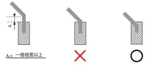
reverse engineer outlet angle of PCB board’s pad is set to avoid the acute angle between the wire and the pad
Modern EDA PCB design copying software (such as Cadence Allegro, Altium Designer, etc.) comes with complete layout routing options.

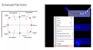
Using Cadence Allegro’s Enhanced Pad Entry function allows us to avoid the acute angle between the circuitry wire and the pad when the wire exits, and avoid the “acid traps” DFM problem.
We use these auxiliary options flexibly in electronic circuit board layout re-routing, which can greatly avoid our production during layout. “acid trap” phenomenon Setting the exit angle of the pad to avoid the acute angle between the wire and the pad.
Using Cadence Allegro’s Enhanced Pad Entry function allows us to avoid the angle between the wire and the pad when the wire exits as much as possible during the layout, and avoid the “acid traps” design for manufacturing problem.

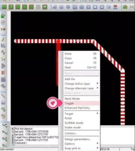
Use Cadence Allegro flexibly to switch the “toggle” option when wiring, which can avoid the acute angle formed when the wire is pulled out of the T-shaped branch, and avoid the “acid traps” DFM problem


