With the rise of the Internet of Things technology, it is becoming more and more common for electronic products to carry wireless communication functions. The wireless communication technology relies on the Radio Frequency Module PC Board to achieve and requires professional design and simulation analysis tools. As a result of that, Reverse Design Radio Frequency Module PC Board Wiring Schematic is growing more and more important in these days reverse engineering printed circuit board technology;

For the Radio Frequency Module Circuit Board layout without its own connector, it needs to be connected to the antenna feed point or connector through the RF trace.
For the Radio Frequency Module Circuit Board layout without its own connector, it needs to be connected to the antenna feed point or connector through the RF trace. Therefore, it is recommended to use the microstrip line for the RF line. The shorter the better, the loss is controlled within 0.2dB, and the impedance is controlled at 50Ω.
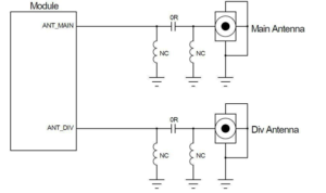
Reserve a π-type circuit between the module and the antenna connector (or feed point) (the ground pins of the two parallel devices should be directly connected to the main ground) for antenna debugging.
When electronic PCB board rerouting, this signal routing controls 50Ω. The RF performance of the product is closely related to this trace. The factors affecting the impedance of this trace on the PCB are as follows:
The width and thickness of the trace
Dielectric constant and thickness
The thickness of the pad
Distance to ground
Nearby wiring

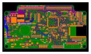
Reverse Design Radio Frequency Module PC Board Wiring Schematic


