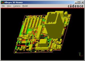
Reverse Design PCB Board Structure will be able to draws the PCB board spacial structure in the printed circuit board structural designing environment which is a critical part for reverse engineering circuit board, according to the determined circuit board size and various mechanical positioning on the printed circuit card surface, and place the required connectors, buttons/switches, screw holes, assembly holes, etc.

Reverse Design PCB Board Structure
According to the PC Board component positioning requirements. And fully consider and determine the wiring area domain and non-wiring area (such as how much area around the screw hole belongs to the non-wiring area).
Reverse Design PCB Board Structure is often the first step for everyone to consider when the schematic diagram is transferred to PCB design. It is also a crucial step in printed circuit board layout redesign.
The quality of the structure of the PCB board is even directly related to the cost of the circuit board manufacturing and the quality of the EMC performance. The following briefly introduces the design of PCB stack structure from two aspects of PCB layer estimation and manufacturability.


