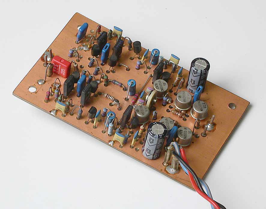
It is a frequent need to have schematic diagram in the industry of PCB Board cloning, repairing and maitenance, especially for those expensive, rare to find or obselete which has already phased out for the production for many years without the possibility to buy the new one. Engineer will normally try to Restore Schematic from Physical Printed Circuit Board in hand and also we can recommend PCB reverse engineering technique for you. hereby we would like to introduce some simple notification for this procedures:

obselete PCB which has already phased out for the production for many years
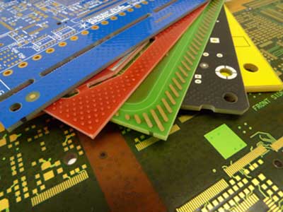
Step 1, Look at the solder mask first, as we all know there are various colors of solder mask will be applied on the PCB board, if the colors are yellow, green or red will be easier to view the circuitry pattern on the physical PC Board, if the solder mask color is black, then it is necessary to scrub the board and strip off the mask.

Sometimes it is not easy to identify the layer count of circuit board. normally single-sided and double-sided will be easier, and if the Printed circuit board is with the multi-layer it would be necessary to remove the TOP & BOTTOM layer before it is possible to get access to the inner layers.
The package of components installed on the PCB board can be DIP inserted mounted or SMD. If most of the components are with surface mounted package, then a proper and good microscope will be required to monitor the circuit layout and wire pattern by reverse engineering PCB.
Then take a multimeter and find a line which extended from a core unit. For example, find the central integrated circuit such as MCU, CPLD or FPGA model number, and learn the schematic diagram of it through datasheet found from the Internet search, corresponding to looking for components on the circuit board. Even if you can’t draw a schematic, you can know the function by finding the chip model and schematic.


