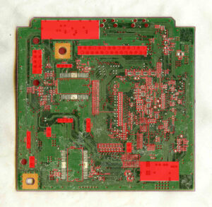
Sometimes the purpose of reverse engineering PCB board not only to cloning original electronic circuit board, but also want to further increase the function, which directly increases the difficulty on the PCB layout design. If you increase it through the schematic part, then things will be much simpler, that is one of the main reason why we need to Restore Electronic Circuit Board Schematic Diagram.
Next, let’s discuss the process of restoring the PCB layout of the product into a schematic diagram
(1) Export the netlist file (test. net) of this PCB layout through CAD software Protel 99se.
(2) Open the program Omninet for Windows, set the input file type to Protel, the input file to test.net, the output file type to EDIF, the output file name is test.edf, then run it, open test.edf, right-click and select Generate Schamatics, after successful recognition, select Orcad9.10 as the save file type.

Restore Electronic Circuit Board Schematic Diagram
(3) Open this file in ORCAD and save it as protel format, so that CAD software Protel 99se or Protel 2004 can be directly applied
(4) At this point, we can directly edit and modify the schematic part. We can add the circuit part corresponding to the product to be added to the schematic part, and then re-layout the PCB layout (number of layers, lines Width, line spacing, routing mode, etc.).
The layout of the layout can be said to be very important. If the analog signal is not wired separately from the digital signal or the high-frequency and low-frequency parts, the performance of the product will be greatly affected. Therefore, the wiring needs to follow the relevant rules and complete the model After that, you need to use the equipment to test the relevant parameters to see if they meet the requirements or what problems exist. The parameters are not modified.


