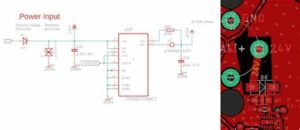
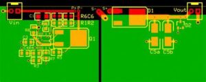
Reroute Multilayer PCB Board Layout Design can help to not only minimizes the loop area between the power supply and ground, but also reduces the high-frequency EMI electromagnetic field generated by the ESD pulse. If a multi-layer circuit board cannot be used, the wires for power and ground must be connected in a grid as shown in below Figure.

If a multi-layer circuit board cannot be used, the wires for power and ground must be connected in a grid
The grid connection can play the role of power supply and ground layer. The vias are used to connect the printed wires of each layer. The via connection interval should be within 6 cm in each direction. In addition, when wiring PCB layout and gerber file, placing the power supply and ground trace as close as possible can also reduce the loop area, as shown in below Figure.

Reroute Multilayer PCB Board Layout Design
Another way to reduce loop area and induced current is to reduce parallel paths between interconnected devices.
When a signal connection line longer than 30 cm must be used, a protection line can be used. A better approach is to place a ground layer near the signal line. The signal line should be within 13 mm from the protective line or ground layer, the long signal line (>30 cm) or power supply line of each sensitive element and its ground line are arranged crosswise. The crossing lines must be arranged at regular intervals from top to bottom or from left to right.


