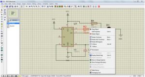
Relayout Electronic PCB Board Circuitry Diagram is necessary for other obsolete circuit board due to the END OF LIFE components used on it which will required to replace with alternatives or improve the electrical/electronic performance stability, modification over the current printed circuit board schematic diagram and layout drawing;

Relayout Electronic PCB Board Circuitry Diagram is necessary for other obsolete circuit board due to the END OF LIFE components used on it which will required to replace with alternatives or improve the electrical/electronic performance stability, modification over the current printed circuit board schematic diagram and layout drawing
B. Layout
1. Set the size of the board frame according to the structure drawing, arrange the mounting holes, connectors and other components that need to be positioned according to the structural elements, and give these components immovable attributes.
Carry out dimension analysis and marking according to the requirements of process redesign specifications.
2. Set the forbidden wiring area and the forbidden layout area of the printed circuit board according to the PCB circuit board structure drawing and the clamping edge required during production and processing. According to the special requirements of some components, set up no wiring area.
3. Comprehensive consideration of PCB performance and processing efficiency to select the pcb board cloning processing flow. The preferred sequence of the processing technology is: single-sided mounting on component side-component side mounting, insert and mixed mounting (component side mounting and soldering surface mounting once wave forming)-double side mounting-component side mounting and insert mixed mounting Soldering surface mount.
4. Basic principles of layout operation
A. Follow the layout principle of “big first, then small, difficult first, easy later”, that is, important unit circuits and core components should be laid out first.
B. The principle block diagram should be referred to in the layout, and the main components should be arranged according to the main signal flow of the board.
C. The layout should meet the following requirements as far as possible: the total connection is as short as possible, and the key signal line is the shortest; high voltage, large current signal and low current, low voltage weak signal are completely separated; analog signal and digital signal are separated; high frequency signal Separate from low-frequency signals; the spacing of high-frequency components should be sufficient.
D. For circuits with the same structure, adopt a “symmetrical” standard layout as much as possible;
E. Optimize the layout according to the standards of uniform distribution, balanced center of gravity, and beautiful layout;
F. Device layout grid setting. In general IC device layout, the grid should be 50-100 mil. For small surface mount devices, such as surface mount component layout, the grid setting should be no less than 25mil.
G. If there are special layout requirements, they should be determined after communication between the two parties.


