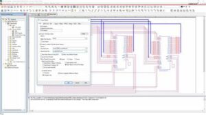
Recreate Printed Circuit Board Netlist Drawing is step taken after get the BILL OF MATERIAL ready, so the component arrangement of printed wiring board can be replicated after desolder each one of them off the board, and then prepare the Bill of material list from physical PCB board sample;

Recreate Printed Circuit Board Netlist Drawing is step taken after get the BILL OF MATERIAL ready, so the component arrangement of printed wiring board can be replicated after desolder each one of them off the board, and then prepare the Bill of material list from physical PCB board sample
A. Recreate a netlist
1. The network table is the interface file between the schematic diagram and the PCB layout drawing. The PCB designer should select the correct network table format according to the schematic diagram and the characteristics of the PCB design tool used, and create a network table that meets the requirements.
2. In the process of creating the netlist, according to the characteristics of the schematic design tool, actively assist the schematic designer to eliminate errors. Ensure the correctness and completeness of the netlist.
3. Determine the package of the device (PCB FOOTPRINT).
4. Create PCB board Create a PCB design file according to the board structure diagram or the corresponding standard board frame; pay attention to the correct selection of the position of the origin of the board coordinate, and the principle of origin setting:
A. The intersection of the left and lower extension lines of the veneer.
B. The first pad at the bottom left corner of the board. Rounded corners around the frame, with a chamfering radius of 5mm.
Refer to structural design requirements for special circumstances.


