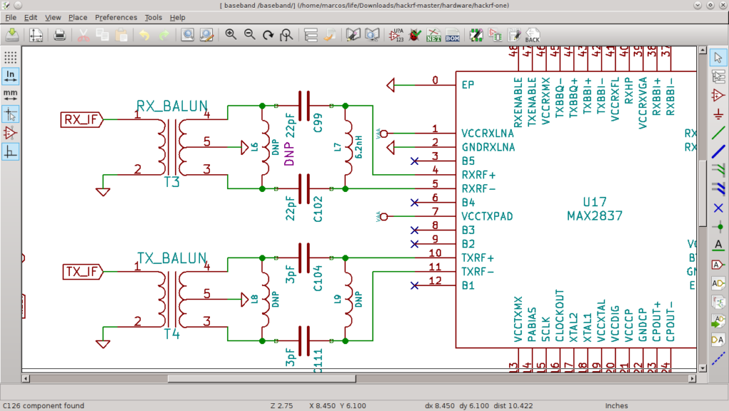
Recover PCB Board Schematic Diagram Purpose project comes from the National Innovation Fund and the “PCB-reverse-engineering-based electronic equipment maintenance technology platform” project supported by the National Defense Research Institute. It is dedicated to solving the current situation that the electronic equipment is damaged and not repaired in time due to the lack of schematic diagram.

At present, there are a large number of electronic devices that exceed the warranty period or have no maintenance guarantee at all. Since the current imported equipment PCB Board does not come with a circuit schematic, or is damaged or the content is inaccurate, it poses a fundamental obstacle to the self-maintenance and spare parts.
Despite advances in electronic repair technology such as fujitsu converter pcb board repair, it is still impossible to change the status quo: advanced electronic equipment with a value of tens of thousands of dollars can be seen in idle or faulty operations; production losses caused by production line downtime are actually occurring every day all provide sufficient proof to support urgency of PCB Board Schematic Diagram recovering.
Effective PCB card recovering in the absent of schematic diagram will provide a great and positive impact on the resulting economic waste and environmental pollution. The first step in reducing costs and reducing pollution is to re-use PCB board what can be repaired, which is also in line with the requirements of a conservation-oriented society proposed by China.
In the process of introducing advanced electronic equipment from abroad, the total amount of damage to various circuit boards is also increasing. Experience tells us that these faulty boards, as long as they have schematics will become much easier to repair.
However, many equipments have lost the schematic diagram because of the long-term. From the maintenance theory, the schematic diagram is the basic information for the maintenance operation. Once the schematic diagram is obtained, the test and maintenance plan and analysis element can be formulated according to the existing conditions. Causes of device damage and suggestions for improvement.


