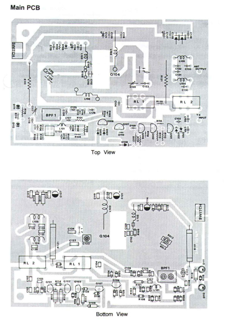
The reconfigurable broadband software radio transceiver circuit board reverse engineering explores issues related to PCB board design.

Firstly, this paper analyzes the structure and working principle of common RF receivers, and introduces a broadband RF and high-speed digital hybrid circuit board design.
Then, the structure of the Radio Transceiver Circuit Board is studied from the perspective of the PCB designer. The relationship between the dielectric constant and dielectric loss tangent of the dielectric layer material and the characteristic impedance, signal propagation speed and energy loss of the transmission line in the PCB are analyzed.
Some issues to be aware of when designing PCB stack-up structure and dielectric layer materials, and summarizing some of the experience and rules of Radio Transceiver Circuit Board Reverse Engineering.
Then, the impedance matching problems encountered in RF circuit design and the problems related to microstrip lines are analyzed and studied. The physical meaning of scattering parameters is discussed. The common performance indexes of RF amplifiers are analyzed. The broadband RF of this design is introduced in depth. The eight-band preselector in the transceiver unit is simulated and analyzed.
Finally, the two important signal integrity problems of reflection and crosstalk in high-speed digital signal PCB reverse engineering are analyzed and studied. The signal integrity problems related to DDR2 SDRAM in the data storage unit of this design are discussed. Emulation termination design method base upon signal integrity has been introduced.


