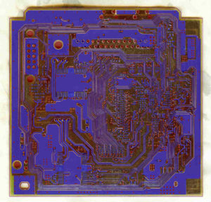
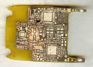
Processing Reverse Engineering PCB Board Data which has been collected through desolder components off the printed circuit board, and scrub the solder mask layer off the top and bottom layer to get the circuitry pattern fully exposed;

Processing Reverse Engineering PCB Board Data which has been collected through desolder components off the printed circuit board, and scrub the solder mask layer off the top and bottom layer to get the circuitry pattern fully exposed
This part is mainly to prepare various data for the subsequent printed circuit board photocopying,
Such as the number of line widths on the circuit board, the width of each line, the size and number of pads, and the packaging form of components.
(1) When we remove all the components on the circuit board, and scan both the front and back sides of the printed circuit board through the scanner and save it in BMP or JPG format (as shown in below Figure),

Next, we can remove the solder resist ink on the board surface by milling machine, chemical corrosion, tool peeling, sandpaper, etc. until the copper foil is exposed (if the wiring density of the circuit board is not large, this step may not be necessary).
(2) Place the circuit board under the microscope to observe and record the relevant information such as the width of the wire, the diameter of the pad, the size of the hole and so on.
(3) According to the device removed from the circuit board, use a vernier caliper to measure the positional relationship between the appearance of the device and the pins to determine what the package of the device is. Then now we have to create a new package in advance.


