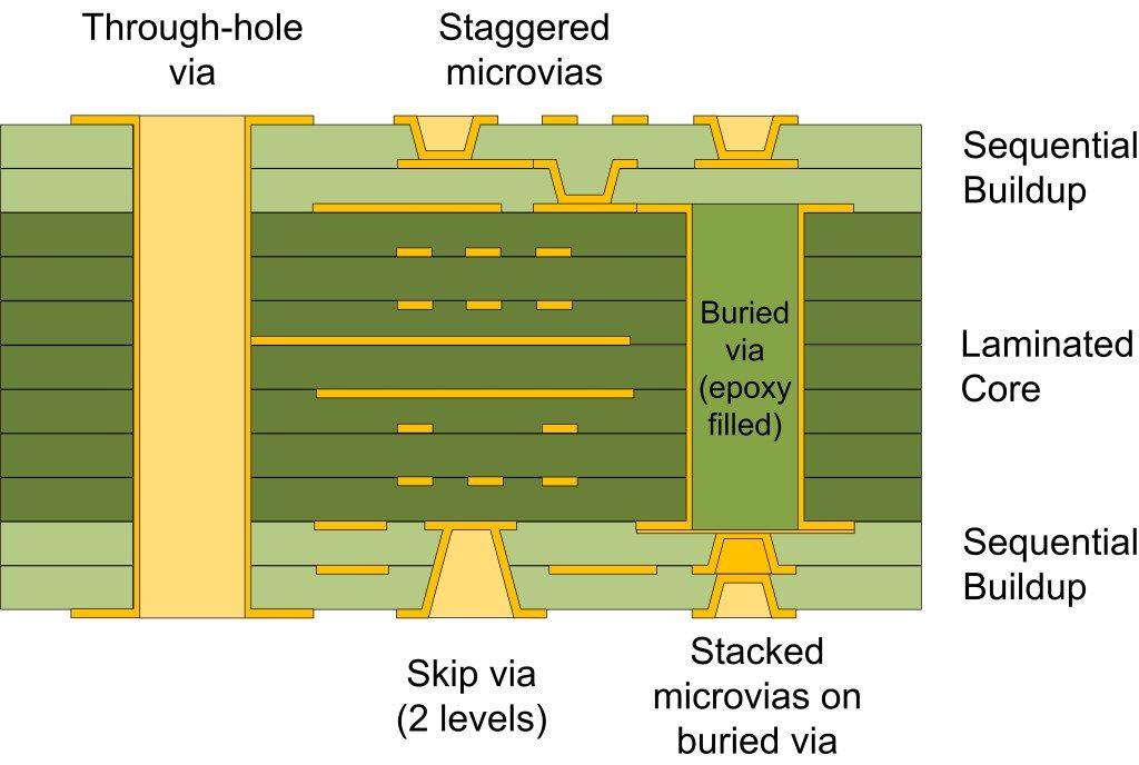
Since the 1990s, more and more chips have been packaged in BGA (ball array) packages, and as technology continues to evolve, the Pitch (the center distance between solder balls and solder balls) of the package has become smaller and smaller. In this case, the solder balls located in the inner layer of the chip are not likely to be routed from the “aisle” between the solder balls PAD on the surface of the PCB. Therefore, the Printed Circuit Board Vias must be used to connect the solder balls to other conductive layers of the PCB. There are 3 types of holes, which are through holes, blind holes and buried holes, as show in below picture:

Among them, the through hole is the simplest through hole, which runs through all the layers of the PCB; it is widely used because of its easy process and low production cost. A blind hole is a through-hole that extends only through the surface of the PCB to the inner conductive layer, just like the elevator access from the top floor (or the ground floor) to the middle floor in the same building.
A buried via is a via that has both an origin and an end point in the inner conductive layer. The use of blind vias and buried vias can greatly optimize PCB layout and reduce PCB area. Because they are not like through-holes, once this position of all layers can no longer be wired or placed (except for the same network), the space that can be routed or placed is reserved for the layers that are not penetrated.


