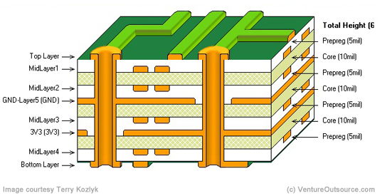
Printed circuit board structure is mainly composed of pads, vias, mounting holes, wires, components, connectors, pads, electrical boundaries, and the like. The most commonly see printed circuit board laminated structures include Single Layer PCB, Double Layer PCB, and Multi-Layer PCB.

The main functions of each component are as follows:
Pad: A metal hole used to solder the component leads.
Via: There are metal vias and non-metal vias, where metal vias are used to connect the component leads between the layers.
Mounting hole: used to fix the board;
Wire: An electrical network copper film used to connect component leads;
Connector: A component used to connect between boards or any other external accessories;
Filling: Copper for the grounding network can effectively reduce the impedance;
Electrical Boundary: Used to determine the size of the board, and all components on the board must not exceed this boundary and this is a very critical point when reverse engineering PCB


