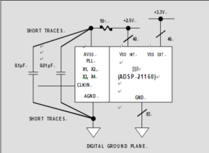
As if dealing with mixed-signal ICs with AGND and DGNDs wasn’t enough in the process of Printed Circuit Board Reverse Engineering, DSPs such as the ADSP-21160 SHARC with internal phase-locked-loops (PLLs) raise issues with respect to proper grounding. The ADSP-21160 PLL allows the internal core clock (determines the instruction cycle time) to operate at a user selectable ratio of 2, 3, or 4 times the external clock frequency, CLKIN. The CLKIN rate is the rate at which the synchronous external ports operate. Although this allows using a lower frequencyexternal clock, care must be taken with the power and ground connections to the internal PLL as shown in below Figure.

Grounding DSPs with Internal Phase-Locked-Loops (PLLs)
In order to prevent internal coupling between digital currents and the PLL, the power and ground connections to the PLL are brought out separately on pins labeled AVDD and AGND, respectively. The AVDD +2.5 V supply should be derived from the VDD INT +2.5 V supply using the filter network as shown. This ensures a relatively noise-free supply for the internal PLL. The AGND pin of the PLL should be connected to the digital ground plane of the PC board using a short trace. The decoupling capacitors should be routed between the AVDD pin and AGND pin using short traces.

DSP Application in Printed Circuit Board Reverse Engineering


