Printed Circuit Board Reverse Design Principle will refers to the tools and facilities which are going to be used for measuring and extracting the information about target printed circuit board;

Reverse Design Principle will refers to the tools and facilities which are going to be used for measuring and extracting the information about target printed circuit board;
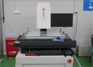
In the preliminary reverse design research process of the circuit board, the designer first solves the outer surface measurement of the circuit board. The methods include coordinate measuring instrument, laser line scanning measurement, vernier caliper measurement, spiral micrometer, etc.

the designer first solves the outer surface measurement of the circuit board
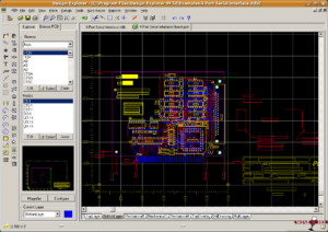
For the measurement of the inner layer circuitry pattern of printed circuit board, first of all, the circuit and substrate of the outer layer of the circuit board should be stripped off by the grinding method, and then scanned by the scanner to extract the circuitry pattern information of the inner layer. When all the layers’ images have been extracted, And after scanning, the layout and schematic diagram drawing data is extracted in the printed circuit board reverse design software, and after the stacking process, it is imported into the circuit CAD software.


