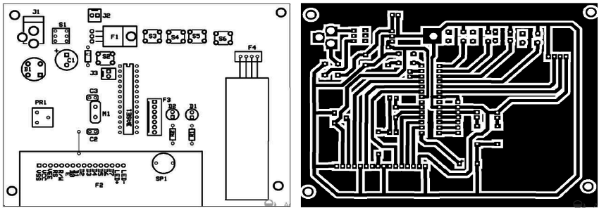
Printed circuit board Principle is to isolate the surface copper foil conductive layer by using the board-based insulating material, so that the current flows along various pre-designed routes in various components such as power consumption, amplification, attenuation, modulation, demodulation, and coding. And other functions.

On the most basic aspect of PCB, the parts are concentrated on one side and the tracks are concentrated on the other side. Since the wire only appears on one side, this PCB is called a single layer PCB Board. Multilayer boards, with multiple layers of wires, must have appropriate electrical connections between the two layers. The bridge between such circuits is called a via. The basic design process of a printed circuit board can be divided into the following four steps:
(1) The design of the circuitry schematic diagram—The design of the circuit schematic diagram is mainly to draw the schematic diagram by using the schematic editor of Protel DXP.
(2) Generate network report—Network report is a report showing the relationship between circuit principle and each component. It is the bridge and link connecting the circuit schematic diagram design and PCB design, and the network report through the circuit schematic diagram. The connection between components can be quickly found to facilitate the design of the upcoming PCB.
(3) Design of printed circuit board—The design of printed circuit board is what we usually call PCB design, which is the final form of circuit schematic conversion. The design of this part is larger than the design of circuit schematic. Difficulty, we can use the powerful design features of Protel DXP to complete this part of the design.
(4) Generate printed circuit board report — After the printed circuit board design is completed, it is necessary to generate various reports, such as generating pin report, circuit board information report, network status report, etc., and finally printing the printed circuit board layout diagram.


