“Noise problem!” – This is the problem that every PCB Board engineer will hear. In order to solve the noise problem, it often takes several hours to carry out laboratory tests in order to find out the culprit, but in the end, it is found that the noise is caused by improper PCB layout of the switching power supply. Solving such problems may require printed circuit board layout redesign, resulting in product delays and increased development costs.

printed circuit board layout redesign
This article will provide guidance on the printed circuit board layout redesign to help designers avoid such noise problems. As an example, the switching regulator layout uses the dual channel synchronous switching controller ADP1850. The first step is to determine the current path of the regulator. The current path then determines the position of the device in the low noise layout design.
The first step of redesigning printed circuit board layout to reduce the noise: Determine the current path
In a switching converter design, the high current path and the low current path are very close to each other. The alternating current (AC) path carries spikes and noise, the high direct current (DC) path produces a considerable voltage drop, and the low current path is often sensitive to noise. as a result of that, the key to redesign a proper PCB layout is to identify critical paths, then arrange the device and provide enough copper area to avoid high currents from damaging low currents.
Poor performance is grounded bounce and noise injection into the IC and the rest of the system from the ground path.
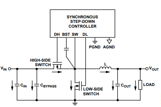
Below Figure shows a synchronous buck regulator design that includes a switching controller and the following external power devices: high-side switches, low-side switches, inductors, input capacitors, output capacitors, and bypass capacitors. The arrows in Figure 1 indicate the flow of high switching currents. Care must be taken to place these power devices to avoid undesirable parasitic capacitance and inductance, resulting in excessive noise, overshoot, ringing, and ground bounce.

Switched current paths such as DH, DL, BST, and SW must be properly routed away from the controller to avoid excessive parasitic inductance. The high δI/δt AC switching pulse currents carried by these lines may reach more than 3 A and last for a few nanoseconds. The high current loop must be small to minimize output ringing and avoid picking up extra noise.
Low-value, low-amplitude signal paths, such as compensation and feedback devices, are sensitive to noise. These paths should be kept away from the switching nodes and power devices to avoid injecting interference noise.


