

Printed Circuit Board (PCB) Layout Optimization is a critical aspect of designing and enhancing Programmable Logic Controller (PLC) PCBs used in robotic arms. These specialized electronic circuit boards must efficiently handle complex control algorithms, real-time data processing, and high-speed communication between sensors, actuators, and motor drivers. Due to their role in ensuring precise robotic movement, optimizing the PCB layout is crucial to prevent signal interference, enhance durability, and maintain system reliability.
Optymalizacja układu PCB jest krytycznym aspektem projektowania i ulepszania PCB sterowników PLC (Programmable Logic Controller) stosowanych w ramionach robotów. Te specjalistyczne płytki elektroniczne muszą sprawnie obsługiwać złożone algorytmy sterowania, przetwarzanie danych w czasie rzeczywistym i szybką komunikację między czujnikami, siłownikami i sterownikami silników. Ze względu na ich rolę w zapewnianiu precyzyjnego ruchu robota, optymalizacja układu PCB jest kluczowa dla zapobiegania zakłóceniom sygnału, zwiększania trwałości i utrzymywania niezawodności systemu.
Unique Features of PLC PCBs in Robotic Arms
A PLC PCB in a robotic arm acts as the central processing unit, interpreting input signals from various sensors and executing predefined control sequences. These PCBs incorporate:
-
High-speed signal processing: PLC PCBs often feature FPGA chips, microcontrollers, and real-time processors to manage motion control in milliseconds.
-
Multiple communication interfaces: These boards support CAN bus, RS-485, Ethernet, and industrial protocols to interact with external systems and coordinate with other machinery.
-
High voltage and current handling: Robotic arms require powerful motor drivers and relay circuits, making PCB layout optimization essential for managing power distribution efficiently.
-
Mixed-signal design: PLC PCBs combine digital control circuits with analog feedback loops, making it essential to separate power, ground, and signal traces to minimize crosstalk and noise.
-
Redundancy and fault tolerance: Many robotic applications require fail-safe mechanisms, where the PCB integrates backup systems or self-recovery circuits to prevent failure during operation.
Reverse engineering a PLC PCB in a robotic arm presents significant difficulties due to its intricate design and proprietary architecture. Some key challenges include:
-
Оптимизация компоновки печатной платы (PCB) является критически важным аспектом проектирования и усовершенствования печатных плат программируемых логических контроллеров (ПЛК), используемых в роботизированных манипуляторах. Эти специализированные электронные платы должны эффективно обрабатывать сложные алгоритмы управления, обработку данных в реальном времени и высокоскоростную связь между датчиками, исполнительными механизмами и драйверами двигателей. В связи с их ролью в обеспечении точного движения робота, оптимизация компоновки печатной платы имеет решающее значение для предотвращения помех сигнала, повышения долговечности и поддержания надежности системы.
Complex Multi-layer Routing
Many PLC PCBs have multi-layer stack-ups to accommodate high-density interconnects. Extracting accurate Gerber files, netlists, and layout drawings from such designs can be difficult, especially when inner layers are buried. -
Encrypted Firmware and Proprietary Components
PLC boards often contain custom firmware stored in microcontrollers or FPGAs, making it difficult to fully replicate or duplicate their functionality without access to the original code. Some manufacturers also use proprietary integrated circuits that are hard to reproduce or remanufacture. -
Signal Integrity and High-Frequency Noise
Since robotic arm controllers process signals at high speeds, poor PCB layout optimization can lead to signal degradation, electromagnetic interference (EMI), and timing issues. Reverse engineering requires careful analysis of trace impedance, ground planes, and shielding techniques. -
Component Miniaturization
Modern PLC PCB boards use surface-mount technology (SMT) with fine-pitch components, making physical measurement and BOM list recovery more challenging. Accurately identifying and sourcing replacement components can be a hurdle when remanufacturing an old or damaged PCB.
La optimización del diseño de las placas de circuito impreso (PCB) es un aspecto fundamental del diseño y la mejora de las PCB de los controladores lógicos programables (PLC) utilizados en brazos robóticos. Estas placas de circuito electrónico especializadas deben gestionar eficientemente algoritmos de control complejos, procesamiento de datos en tiempo real y comunicación de alta velocidad entre sensores, actuadores y controladores de motor. Debido a su papel en la precisión del movimiento robótico, la optimización del diseño de las PCB es crucial para evitar interferencias de señales, aumentar la durabilidad y mantener la fiabilidad del sistema.
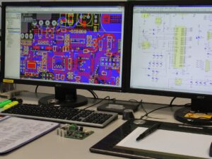
The Printed Circuit Board layout is optimized in terms of grounding, decoupling, and signal routing and can be used as a model when laying out the ADC section of the PC board in a system. The actual evaluation board layout is usually available from the ADC manufacturer in the form of Printed Wiring Board CAD files (Gerber files).
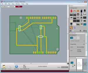
La técnica de ingeniería inversa de la placa PCB implica extraer información de una PCB existente para comprender cómo funciona, identificar sus componentes, rastrear las conexiones y reconstruir su diseño esquemático.
In many cases, the printed circuit board layout of the various layers appears on the data sheet for the device. It should be pointed out, though, that an evaluation board is an extremely simple system. While some guidelines can be inferred from inspection of the layout, the system that you are designing is undoubtedly more complicated. Therefore, direct use of the layout may not be optimum in larger systems.
تتضمن تقنية الهندسة العكسية للوحة ثنائي الفينيل متعدد الكلور استخراج المعلومات من ثنائي الفينيل متعدد الكلور الموجود لفهم كيفية عمله وتحديد مكوناته وتتبع الاتصالات وإعادة بناء تصميمه التخطيطي.
Manufacturers of high performance mixed-signal ICs, like Analog Devices, often offer evaluation boards to assist designers in their initial evaluations and PC Board layout. ADC evaluation boards generally contain an on-board low jitter sampling clock oscillator, output registers, and appropriate power and signal connectors. They also may have additional support circuitry such as the ADC input buffer amplifier and external reference.


