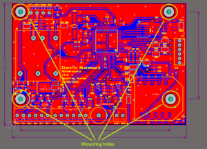
Printed Circuit Board Gerber File Restoration will needs to take the components arrangement/layout into consideration, because the proper component layout will greatly improve the performance of printed circuit boards, especially for those obselete ones which has been designed and layout long time ago, there are several points must be noted when restore PCB board gerber file:

Printed Circuit Board Gerber File Restoration will needs to take the components arrangement/layout into consideration, because the proper component layout will greatly improve the performance of printed circuit boards,
1st:
The same type of plug-in components should be placed in one direction in the X or Y direction. The same type of polarized discrete components should also strive to be consistent in the X or Y direction to facilitate production and inspection.
2nd:
The heating elements should generally be evenly distributed to facilitate the heat dissipation of the veneer and the whole machine. Temperature sensitive devices other than the temperature detection element should be kept away from the components with a large amount of heat.
3rd:
The arrangement of components should be convenient for debugging and maintenance, that is, large components cannot be placed around small components, components to be debugged, and there must be enough space around the components.
4th:
For veneers that need to be produced by wave soldering, the fastener installation holes and positioning holes should be non-metallized holes. When the mounting hole needs to be grounded, it should be connected to the ground plane by means of distributed grounding holes.

For veneers that need to be produced by wave soldering, the fastener installation holes and positioning holes should be non-metallized holes. When the mounting hole needs to be grounded, it should be connected to the ground plane by means of distributed grounding holes.
5th:
When the soldering surface of the mounting components adopts the wave soldering production process, the axis of the resistor and capacitor should be perpendicular to the wave soldering transmission direction, and the axis of the resistor and SOP (PIN spacing greater than or equal to 1.27mm) components are parallel to the transmission direction; Avoid wave soldering for active components such as IC, SOJ, PLCC, QFP, etc. whose PIN pitch is less than 1.27mm (50mil);


