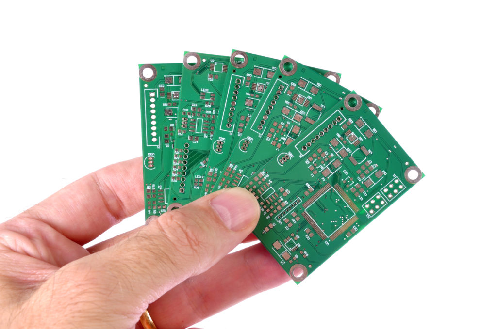
We all know that the manufacturing of PCB Board is the process of reflecting the PCB Board layout design on the physical PCB Board, thus forming a specific industrial product of PCB Board. Printed Circuit Board Copying of the layout design and Gerber file in the market is not directly from the original layout design, but through the process from product to layout design then convert to product.
Because the general pcb design companies use computer tools and auxiliary software to complete the PCB layout design, once the PCB design has been completed, the original pcb layout design documents will be stored in the computer or the corresponding hard disk in the form of electronic data, and a considerable part of them will be also encrypted.

It is almost impossible for other unauthorized 3rd party to get the original layout design in electronic form, but after the pcb board containing the original layout design enters the market, it is very easy for them to obtain the pcb board layout drawing and Gerber file, schematic diagram.
They analyzed the pcb board through reverse engineering technique to obtain relevant technical information such as pcb layout design and gerber file, schematic diagram and Bill of material. The starting point of Printed Circuit Board Copying is the PCB level layout design of the product level – pcb board. To study the intellectual property protection of PCB reverse engineering, we must clarify the current situation of
Printed Circuit Board Copying and the intellectual property issues it involves and be aware that existing law is insufficient for the pcb layout design and pcb board reverse engineering protection at the product level.


