
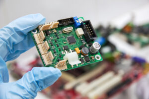
The printed circuit board (PCB) has been the fundamental building block of electronic devices since the dawn of the modern electronic age, shortly after World War II. Its ability to create numerous connections in a single soldering step and its cost-effective mass production have solidified its role in electronics manufacturing. Despite advancements in technology, the PCB remains indispensable, adapting to the ever-growing demands for smaller, faster, and more affordable devices.
L’histoire des circuits imprimés remonte au début du XXe siècle, mais leur adoption généralisée a commencé après la guerre. Les premiers PCB étaient de simples cartes planes constituées de matériaux non conducteurs sur lesquels étaient gravées des pistes de cuivre. Ces pistes étaient connectées à des anneaux autour de trous percés où étaient insérées les broches des composants.
L’électronique a évolué, tout comme la technologie PCB. Le besoin de structures de composants plus petites et plus denses a favorisé des innovations telles que les cartes multicouches, les PCB flexibles et les interconnexions haute densité (HDI). Chaque révolution dans la conception des circuits imprimés a été suivie de périodes de perfectionnement, améliorant la fiabilité et la prévisibilité de la fabrication.
The Origins and Evolution of PCB Technology
The history of printed circuit boards traces back to the early 20th century, but their widespread adoption began in the post-war era. Early PCBs were simple planar boards made of non-conductive materials with copper traces etched onto them. These traces connected to annular rings around drilled holes where component leads were inserted.
As electronics evolved, so did PCB technology. The need for smaller, denser component structures drove innovations such as multilayer boards, flexible PCBs, and high-density interconnects (HDIs). Each revolution in PCB design was followed by refinement periods, improving manufacturing reliability and predictability.
Key Elements in PCB Design and Manufacturing
Modern PCB development relies on several critical files and processes:
- Schematic Diagram: The blueprint of an electronic circuit, defining component connections.
- Layout Drawing: The physical arrangement of traces and components on the PCB.
- Gerber File: The industry-standard format used for PCB fabrication, detailing copper layers, solder masks, and drill paths.
- BOM List (Bill of Materials): A comprehensive list of all components required for assembly.
- Netlist: Defines electrical connections between components.
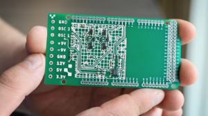
PCB Reverse Engineering and Restoration
प्रिंटेड सर्किट बोर्ड (PCB) द्वितीय विश्व युद्ध के तुरंत बाद, आधुनिक इलेक्ट्रॉनिक युग की शुरुआत से ही इलेक्ट्रॉनिक उपकरणों का मूलभूत निर्माण खंड रहा है। एक ही सोल्डरिंग चरण में कई कनेक्शन बनाने की इसकी क्षमता और इसके लागत-प्रभावी बड़े पैमाने पर उत्पादन ने इलेक्ट्रॉनिक्स निर्माण में इसकी भूमिका को मजबूत किया है। प्रौद्योगिकी में प्रगति के बावजूद, PCB अपरिहार्य बना हुआ है, जो छोटे, तेज़ और अधिक किफायती उपकरणों की लगातार बढ़ती माँगों के अनुकूल है।
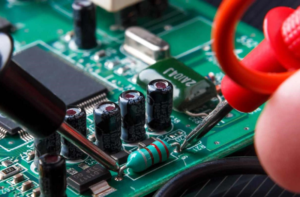
In cases where original documentation is lost or outdated, engineers often recover, restore, or recreate PCBs through reverse engineering. Techniques such as:
- Cloning (replicating an existing PCB)
- Refurbishing (repairing and updating old boards)
- Redesigning (optimizing layouts for modern components)
are employed to remanufacture or reproduce legacy systems. Advanced imaging and scanning technologies allow experts to duplicate or replicate complex PCBs accurately.
The Future of PCBs
Despite emerging technologies like 3D-printed electronics, the PCB remains dominant due to its adaptability. Innovations in materials, such as flexible and stretchable circuits, ensure that PCBs will continue to meet future demands.
Conclusion
From its early beginnings to its current advanced forms, the printed circuit board has proven its resilience. Whether through reverse engineering, redevelopment, or redesign, PCB technology continues to evolve, maintaining its status as the backbone of modern electronics.
By understanding its history and leveraging modern tools like Gerber files, schematic diagrams, and BOM lists, engineers can restore, replicate, and refine PCBs for future generations of electronic devices.
Von ihren Anfängen bis zu ihren heutigen fortschrittlichen Formen hat die Leiterplatte ihre Widerstandsfähigkeit bewiesen. Ob durch Reverse Engineering, Neuentwicklung oder Redesign – die Leiterplattentechnologie entwickelt sich kontinuierlich weiter und behauptet ihren Status als Rückgrat der modernen Elektronik.
Durch das Verständnis ihrer Geschichte und den Einsatz moderner Werkzeuge wie Gerber-Dateien, Schaltplänen und Stücklisten können Ingenieure Leiterplatten für zukünftige Generationen elektronischer Geräte restaurieren, replizieren und optimieren.


