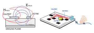
In the process of Printed Circuit Board (PCB) design, ensuring signal integrity is crucial, especially when dealing with high-frequency or high-precision applications that involve both analog and digital signals. One of the most significant challenges engineers face is crosstalk, which occurs when signals interfere with one another due to electromagnetic coupling. This can be particularly problematic in reverse engineering PCB boards, where the original design intent may not be fully documented, making it difficult to optimize signal paths and grounding strategies.
clonar arquivo gerber de placa PCB eletrônica, desenho de layout e lista BOM, diagrama esquemático de engenharia reversa da placa de circuito impresso, copiar placa de circuito impresso por meio desses documentos;
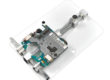
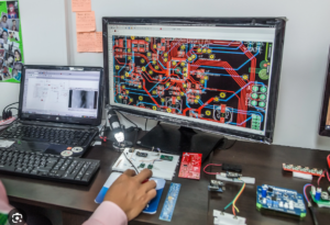
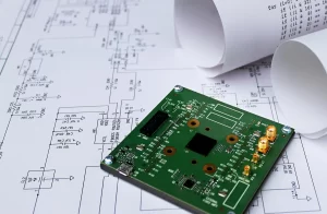
Challenges in PCB Layout and Reverse Engineering
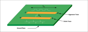
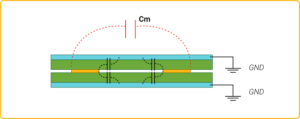
To minimize crosstalk and unwanted interference, PCB layout design must follow strict guidelines. Ideally, sensitive signals should be physically separated as much as possible. However, this is often difficult to achieve, especially when remanufacturing a PCB from an existing board without access to original Gerber files, netlists, or schematic diagrams. In many cases, designers must carefully analyze the PCB board layout to reconstruct an optimized signal path while mitigating design flaws.
Para minimizar la diafonía y las interferencias no deseadas, el diseño de la PCB debe seguir unas directrices estrictas. Idealmente, las señales sensibles deberían estar lo más separadas físicamente posible. Sin embargo, esto suele ser difícil de lograr, especialmente al refabricar una PCB a partir de una placa existente sin acceso a los archivos Gerber, listas de conexiones o diagramas esquemáticos originales. En muchos casos, los diseñadores deben analizar cuidadosamente el diseño de la PCB para reconstruir una ruta de señal optimizada y, al mismo tiempo, mitigar los fallos de diseño.
One of the key principles in PCB reverse engineering is ensuring that high-level analog signals are well-separated from low-level analog signals. Both of these should also be isolated from digital signals, as digital components, particularly TTL and CMOS logic, generate high transient currents that can modulate the ground plane. When a PCB is cloned or modified, failure to account for these high-speed switching characteristics can lead to unexpected performance degradation or signal distortion in the replicated board.
Um dos princípios-chave na engenharia reversa de PCB é garantir que os sinais analógicos de alto nível sejam bem separados dos sinais analógicos de baixo nível. Ambos também devem ser isolados dos sinais digitais, pois os componentes digitais, particularmente a lógica TTL e CMOS, geram altas correntes transitórias que podem modular o plano de aterramento. Quando um PCB é clonado ou modificado, a falha em considerar essas características de comutação de alta velocidade pode levar à degradação inesperada do desempenho ou distorção do sinal na placa replicada.
Clock Jitter and Crosstalk Issues in PCB Manufacturing
Another critical issue in PCB board manufacturing is the impact of sampling clock noise. In waveform sampling and reconstruction systems, the sampling clock—which is a digital signal—is just as vulnerable to noise as any analog signal. Even small amounts of noise on the clock line can introduce phase jitter, which directly reduces the signal-to-noise ratio (SNR) of the sampled data. When reverse engineering a PCB, accurately restoring the original clock distribution network is essential to ensure proper timing and synchronization.
Un autre problème crucial dans la fabrication de circuits imprimés est l’impact du bruit de l’horloge d’échantillonnage. Dans les systèmes d’échantillonnage et de reconstruction de formes d’onde, l’horloge d’échantillonnage, qui est un signal numérique, est tout aussi vulnérable au bruit que n’importe quel signal analogique. Même de faibles quantités de bruit sur la ligne d’horloge peuvent introduire une gigue de phase, ce qui réduit directement le rapport signal/bruit (SNR) des données échantillonnées. Lors de la rétro-ingénierie d’un circuit imprimé, il est essentiel de restaurer avec précision le réseau de distribution d’horloge d’origine pour garantir une synchronisation et une synchronisation correctes.
Additionally, clock driver packages used in clock signal distribution must be carefully managed. When multiple clocks of different frequencies are passed through the same driver package, it can result in excess jitter and crosstalk, ultimately degrading overall system performance. This is particularly relevant when duplicating or remanufacturing PCB boards, as variations in component sourcing or slight changes in PCB layout drawings can introduce unforeseen issues.
استنساخ ملف جربر للوحة PCB الإلكترونية، ورسم التخطيط وقائمة BOM، والرسم التخطيطي الهندسي العكسي للوحة الدوائر المطبوعة، ونسخ لوحة الدوائر المطبوعة من خلال هذه المستندات؛
Understanding and mitigating crosstalk, jitter, and signal integrity issues are fundamental aspects of reverse engineering PCB boards and manufacturing high-performance circuit boards. Whether cloning an existing design, modifying a layout, or restoring a damaged PCB, engineers must pay close attention to signal separation, grounding, and clock distribution. Proper analysis of Gerber data, netlists, and BOM lists is crucial to achieving a high-quality, interference-free PCB design that meets the original specifications.